 ALLPCB


In the world of electronics, printed circuit boards (PCBs) are the foundation of almost every device. While standard PCB sizes often meet the needs of typical projects, there are scenarios where oversized PCB manufacturing and extended PCB sizes are essential. But what exactly are non-standard maximum PCB sizes, and how are they used in large PCB applications? Simply put, these are boards that exceed typical dimensions—often larger than 24 x 24 inches (610 x 610 mm)—designed for specialized uses in industries like aerospace, industrial machinery, and telecommunications. In this blog, we'll dive deep into custom PCB dimensions, the challenges of large PCBs, and their unique applications, providing practical insights for engineers and designers looking to push beyond conventional limits.
What Are Non-Standard Maximum PCB Sizes?
Standard PCB sizes typically range from small boards of a few square inches to medium-sized panels around 18 x 24 inches (457 x 610 mm), as these dimensions fit well within common manufacturing equipment and design constraints. Non-standard maximum PCB sizes, however, go beyond these limits, often reaching dimensions of 24 x 48 inches (610 x 1219 mm) or even larger. These oversized boards are tailored for specific projects where space, functionality, or structural integration demands larger footprints.
The need for extended PCB sizes often arises in applications requiring high power distribution, complex multi-layer designs, or integration into large systems. Manufacturing these boards involves specialized equipment, advanced materials, and precise engineering to ensure reliability despite their scale.
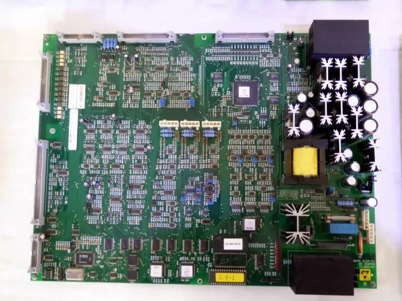
Why Choose Oversized PCB Manufacturing?
The decision to opt for oversized PCB manufacturing isn't taken lightly. These boards are chosen when smaller, standard-sized options can't meet the technical or spatial requirements of a project. Here are some key reasons why engineers turn to large PCB applications:
- High Component Density: Larger boards can accommodate more components or provide better spacing for heat dissipation, critical in high-power systems like industrial control units.
- Simplified Assembly: Using a single large board instead of multiple smaller ones can reduce assembly complexity, minimize connection points, and lower the risk of signal loss or interference.
- Structural Integration: In applications like aerospace or automotive systems, oversized PCBs can be integrated directly into the structural framework of a device, saving space and enhancing durability.
- Power Distribution: Large boards are often used in power electronics, where thick copper layers and wide traces are needed to handle currents exceeding 50 amps or voltages above 500V.
For instance, in renewable energy systems like solar inverters, a single oversized PCB might measure 30 x 40 inches (762 x 1016 mm) to manage high-voltage circuits and integrate multiple control modules. This approach reduces wiring complexity and boosts system efficiency.
Applications of Large PCB Designs
Large PCB applications span various industries, each with unique demands for custom PCB dimensions. Below are some prominent sectors where extended PCB sizes play a critical role:
1. Aerospace and Defense
In aerospace, oversized PCBs are used in radar systems, communication arrays, and satellite equipment. These boards often exceed 36 inches (914 mm) in length to house extensive circuitry for signal processing and power management. For example, a radar control board might require a surface area large enough to support dozens of high-frequency components operating at frequencies above 10 GHz, ensuring minimal signal degradation over long traces.
2. Industrial Automation
Industrial machinery often relies on large PCBs to control complex operations. A factory automation system might use a 24 x 36 inch (610 x 914 mm) board to integrate sensors, motor drivers, and communication interfaces. These boards must withstand harsh environments with temperatures ranging from -40°C to 85°C and vibrations up to 5G, making durability a key design factor.
3. Telecommunications
Telecom infrastructure, such as base stations for 5G networks, frequently employs oversized PCBs to manage high-speed data transmission. These boards can handle signal speeds up to 25 Gbps, requiring precise impedance control (often around 50 ohms for differential pairs) across long distances. A typical board for a 5G antenna array might measure 28 x 48 inches (711 x 1219 mm) to accommodate multiple RF modules.
4. Medical Equipment
Large medical devices like MRI machines or CT scanners use extended PCB sizes to integrate imaging sensors, power supplies, and data processing units. These boards often prioritize signal integrity to avoid noise interference, with trace widths and spacing designed to maintain impedance values within ±10% of the target (e.g., 100 ohms for high-speed signals).

Challenges of Large PCBs: Overcoming the Obstacles
While the benefits of oversized PCB manufacturing are clear, the challenges of large PCBs cannot be ignored. Designing and producing these boards comes with unique hurdles that require careful planning and expertise. Let's explore some of the most common issues:
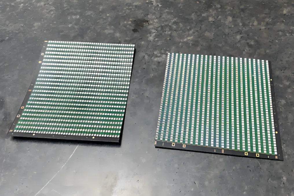
1. Manufacturing Limitations
Standard PCB fabrication equipment is often designed for panels up to 24 x 24 inches (610 x 610 mm). Producing boards beyond these dimensions requires specialized machinery, which can increase costs and lead times. For instance, laminating and drilling processes must maintain precision across a larger surface area, often requiring tolerances as tight as ±0.002 inches (±0.05 mm) to avoid misalignment.
2. Material Warpage and Stress
Larger boards are more prone to warpage due to thermal expansion during manufacturing or operation. Materials like FR-4, commonly used for standard PCBs, may not suffice for oversized designs. Instead, high-Tg (glass transition temperature) materials above 170°C or metal-core substrates are often used to enhance stability. Even then, a board measuring 30 x 50 inches (762 x 1270 mm) might experience bowing up to 0.01 inches (0.25 mm) if not handled properly.
3. Signal Integrity Issues
As PCB size increases, so does the length of traces, which can lead to signal loss or crosstalk. For high-speed applications, maintaining a controlled impedance of 50 ohms across traces longer than 20 inches (508 mm) becomes challenging. Designers often use techniques like back-drilling or adding ground planes to mitigate these issues, but this adds complexity to the layout.
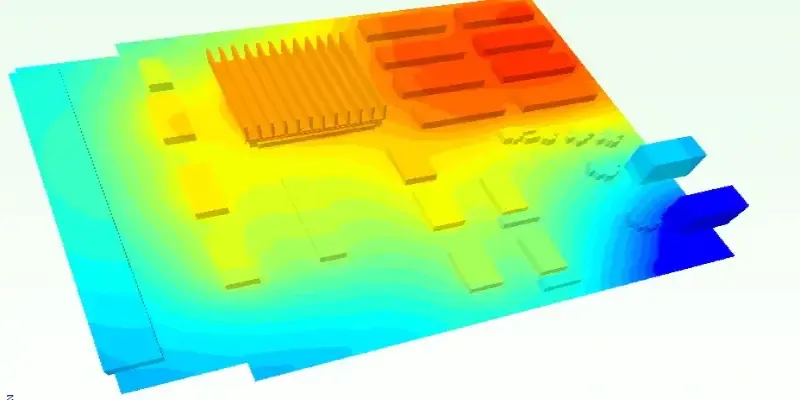
4. Thermal Management
Large PCBs often handle high power, generating significant heat. Without proper thermal design, hotspots can form, leading to component failure. For example, a power distribution board with a current density of 500 A/in2 might require copper thicknesses of 4 oz/ft2 (140 μm) or more, along with heat sinks or vias for heat dissipation.
5. Cost and Logistics
The cost of raw materials, specialized equipment, and shipping for oversized PCBs is significantly higher. A board exceeding 24 x 36 inches (610 x 914 mm) might cost 3-5 times more than a standard-sized equivalent due to these factors. Additionally, transporting and handling such large panels without damage requires custom packaging and careful logistics planning.
Design Tips for Custom PCB Dimensions
Creating a successful oversized PCB requires more than just scaling up a standard design. Here are practical tips to ensure reliability and performance when working with extended PCB sizes:
- Optimize Panelization: Work with your manufacturer to determine the largest panel size their equipment can handle. If a single board exceeds this limit, consider splitting the design into smaller, interconnected panels to reduce manufacturing risks.
- Use Robust Materials: Select materials with low thermal expansion coefficients (CTE) and high mechanical strength. For instance, polyimide or high-Tg FR-4 can withstand the stresses of large boards better than standard laminates.
- Plan for Signal Integrity: Minimize trace lengths where possible and use differential pairs for high-speed signals. Simulate impedance values (e.g., targeting 100 ohms for USB 3.0 signals) during the design phase to avoid surprises.
- Incorporate Thermal Relief: Add thermal vias under high-power components and ensure copper pours are balanced to distribute heat evenly across the board.
- Test and Validate: Before full-scale production, prototype your design to identify potential issues like warpage or signal loss. Testing under real-world conditions (e.g., temperature cycling from -20°C to 80°C) can reveal weaknesses early.
Future Trends in Oversized PCB Manufacturing
As technology advances, the demand for large PCB applications continues to grow. Emerging trends are shaping the future of oversized PCB manufacturing, making it more accessible and efficient:
- Advanced Materials: New substrates like ceramic-filled laminates offer better thermal and mechanical performance for large boards, reducing warpage risks even at sizes exceeding 40 x 60 inches (1016 x 1524 mm).
- Automation in Production: Automated manufacturing systems are being adapted to handle larger panels, improving precision and reducing costs. This could lower the price premium for oversized boards in the coming years.
- 3D Printing Integration: Additive manufacturing techniques are being explored to create complex, large-scale PCBs layer by layer, potentially revolutionizing how custom PCB dimensions are approached.
- IoT and 5G Expansion: The rollout of IoT devices and 5G infrastructure will drive demand for larger boards in smart cities and connected industries, pushing manufacturers to innovate in extended PCB sizes.
Conclusion: Pushing Boundaries with Large PCB Solutions
Non-standard maximum PCB sizes open up a world of possibilities for engineers and designers tackling complex, high-demand projects. From aerospace to telecommunications, oversized PCB manufacturing supports applications where standard boards simply won't cut it. However, the challenges of large PCBs—ranging from signal integrity to thermal management—require careful planning and expertise to overcome. By understanding the unique needs of large PCB applications and leveraging custom PCB dimensions, you can create reliable, high-performance solutions that push beyond conventional limits.


