ALLPCB


In the fast-evolving world of electronics, printed circuit boards (PCBs) are becoming more compact and complex, especially with high-density designs. Traditional silkscreen printing, while widely used for marking components and legends on PCBs, often falls short in meeting the precision and durability needs of modern boards. So, what are the advanced PCB marking alternatives for high-density PCB identification? This blog explores cutting-edge techniques like direct legend printing and laser marking, compares them to silkscreen methods, and addresses component marking challenges to help engineers and designers make informed decisions.
Whether you're dealing with tight spacing on a high-density board or seeking durable marking solutions for harsh environments, understanding these advanced methods can elevate your PCB design and manufacturing process. Let’s dive into the details of these innovative approaches and see how they can benefit your projects.
Why Move Beyond Traditional Silkscreen for PCB Marking?
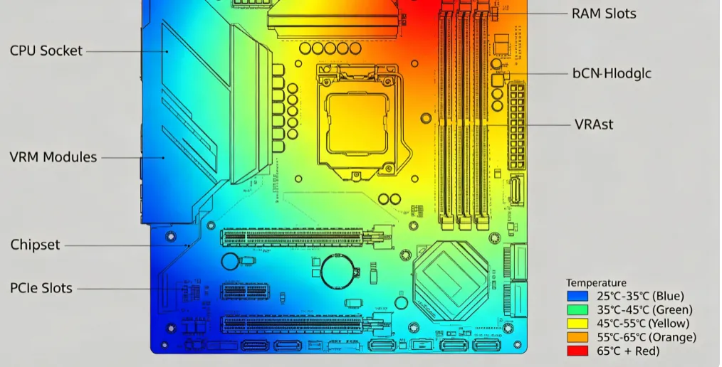
Silkscreen printing has been a staple in PCB manufacturing for decades. It involves applying a layer of non-conductive ink to label components, test points, and other critical information on the board's surface. While effective for simpler designs, silkscreen struggles with the demands of high-density PCBs. These boards often feature components packed closely together, leaving little room for clear markings with line widths below 4 mils (0.1 mm). Additionally, silkscreen ink can wear off under harsh conditions like high temperatures or chemical exposure, leading to identification issues during assembly or repair.
As PCB designs push the boundaries of miniaturization—with trace widths as narrow as 2 mils (0.05 mm) and component densities exceeding 100 components per square inch—there’s a growing need for more precise and durable marking solutions. Advanced techniques like direct legend printing and laser marking offer better resolution, durability, and flexibility for high-density PCB identification. Let’s explore these alternatives and how they address the limitations of silkscreen.
Direct Legend Printing: Precision for High-Density Designs
Direct legend printing (DLP) is an advanced PCB marking technique that uses inkjet technology to apply labels directly onto the board’s surface. Unlike silkscreen, which relies on stencils and can struggle with fine details, DLP offers exceptional precision, capable of producing line widths as small as 2 mils (0.05 mm). This makes it an ideal choice for high-density PCB identification where space is limited, and clarity is critical.
Advantages of Direct Legend Printing Over Silkscreen
- Higher Resolution: DLP can achieve finer details, ensuring legible markings even on boards with component spacing under 0.5 mm.
- Customization: Since it’s a digital process, DLP allows for quick design changes without the need for new stencils, reducing lead times in prototyping phases by up to 30%.
- Reduced Errors: The automated nature of inkjet printing minimizes human error compared to manual silkscreen setups, improving consistency across batches.
Limitations of Direct Legend Printing
While DLP excels in precision, it may not be as durable as other methods. The ink used in DLP can fade under extreme conditions, such as prolonged exposure to temperatures above 150°C or harsh solvents. For applications requiring long-term durability, additional protective coatings may be necessary, increasing costs by approximately 10-15% per board.
For engineers working on consumer electronics or prototypes, direct legend printing vs silkscreen often comes down to a trade-off between precision and durability. If your project prioritizes clarity on high-density boards over ruggedness, DLP is a strong contender.
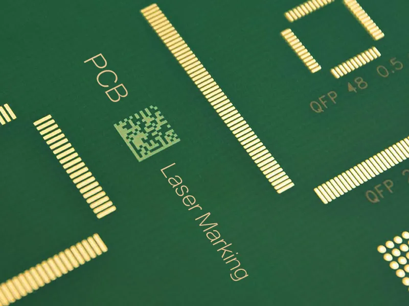
Laser Marking PCB: Durability and Versatility Combined
Laser marking is another powerful alternative for PCB marking, especially for high-density designs and harsh environments. This technique uses a high-energy laser beam to etch or discolor the board’s surface, creating permanent markings without the need for ink. Laser marking machines can achieve resolutions down to 1 mil (0.025 mm), making them suitable for even the most compact PCB layouts.
Key Benefits of Laser Marking for PCBs
- Permanence: Unlike ink-based methods, laser markings are resistant to wear, chemicals, and temperatures up to 200°C, ensuring long-term legibility in industrial or automotive applications.
- Speed: Laser systems can mark boards at rates of up to 100 characters per second, significantly reducing production time for large batches.
- Versatility: Laser marking can be applied to various materials, including FR4, ceramics, and metal-clad boards, offering flexibility across different PCB types.
Challenges with Laser Marking
Despite its advantages, laser marking comes with some drawbacks. The initial investment for laser equipment can be high, often exceeding $50,000 for industrial-grade systems, which may not be feasible for small-scale manufacturers. Additionally, laser marking can sometimes damage the board’s surface if not calibrated properly, potentially affecting solder mask integrity or creating micro-cracks in substrates with low thermal resistance.
For projects where durability and precision are non-negotiable, laser marking PCB technology stands out as a top choice. It’s particularly effective for high-density boards used in aerospace or medical devices, where component identification must remain intact under extreme conditions.
Direct Legend Printing vs Silkscreen: A Side-by-Side Comparison
Choosing between direct legend printing and silkscreen often depends on the specific needs of your PCB project. Below is a detailed comparison to help you decide which method suits your high-density board requirements.
| Feature | Direct Legend Printing | Silkscreen |
|---|---|---|
| Resolution | High (down to 2 mils) | Moderate (minimum 4 mils) |
| Durability | Moderate (may fade without coating) | Low (prone to wear in harsh conditions) |
| Cost | Moderate (10-15% higher with coatings) | Low (cost-effective for simple designs) |
| Speed | Fast (digital process, no stencil setup) | Slower (requires stencil preparation) |
| Best For | High-density PCBs, prototypes | Simple designs, low-cost projects |
From this comparison, it’s clear that direct legend printing offers superior precision and speed, making it a better fit for modern, compact designs. However, silkscreen remains a viable option for budget-conscious projects with less stringent marking requirements.
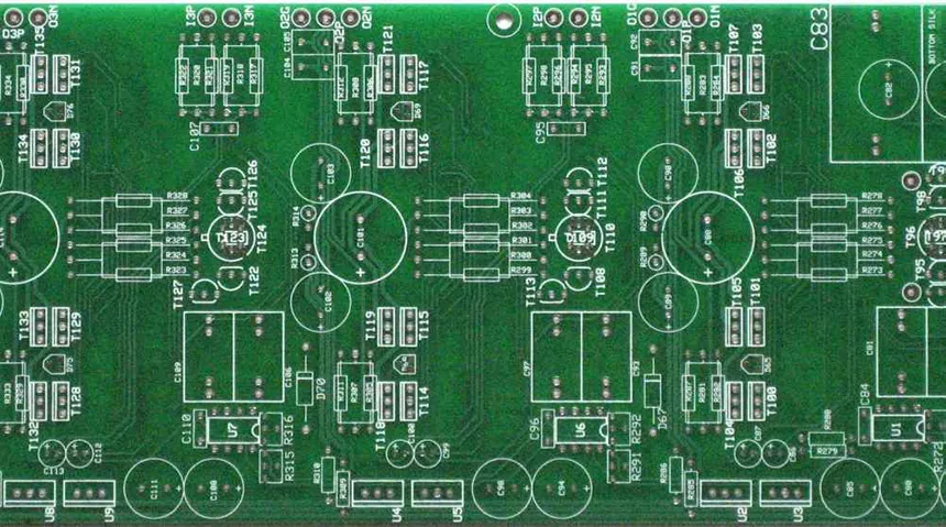
Component Marking Challenges on High-Density PCBs
High-density PCBs present unique component marking challenges that traditional methods like silkscreen often can’t overcome. As boards shrink in size while accommodating more components—sometimes over 200 per square inch—marking space becomes a scarce resource. Here are some of the most common challenges and how advanced techniques address them.
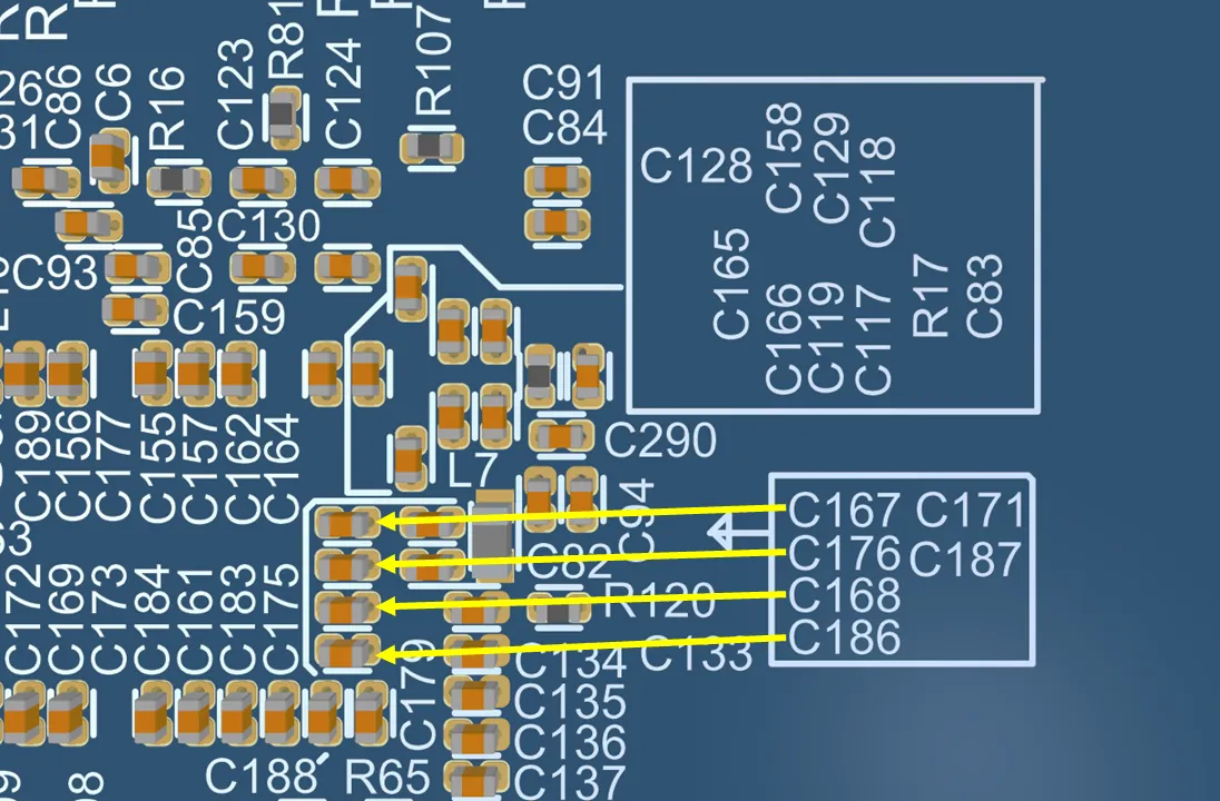
Space Constraints
With component pitches as tight as 0.4 mm in high-density designs, there’s often no room for traditional silkscreen labels. Advanced methods like laser marking and direct legend printing can place micro-text or symbols in areas smaller than 1 mm2, ensuring critical information like polarity markers or component IDs remains visible.
Readability Issues
Smaller markings can become illegible if the resolution isn’t high enough. Silkscreen struggles to maintain clarity below 4 mils, whereas DLP and laser marking can produce crisp text and symbols at 2 mils or less, improving readability during assembly and troubleshooting.
Durability in Harsh Environments
High-density PCBs are often used in demanding applications, such as automotive systems where temperatures can exceed 125°C. Ink-based markings may degrade, leading to identification errors. Laser marking offers a solution by creating permanent etchings that withstand extreme conditions without additional protective layers.
Choosing the Right PCB Marking Alternative for Your Project
Selecting the best marking technique for your high-density PCB depends on several factors, including budget, application environment, and design complexity. Here’s a quick guide to help you decide:
- Budget-Friendly Needs: If cost is a primary concern and your PCB design isn’t overly complex, traditional silkscreen may still work, especially for line widths above 4 mils.
- Precision-Driven Projects: For high-density boards with tight spacing, direct legend printing provides the fine resolution needed for clear markings, ideal for consumer electronics or prototypes.
- Durability Requirements: If your PCB will face harsh conditions, such as high heat or chemical exposure, laser marking is the go-to choice for permanent, reliable identification.
By aligning the marking method with your project’s specific needs, you can optimize both performance and cost-effectiveness. For instance, a medical device manufacturer might invest in laser marking for its durability, while a startup developing IoT gadgets might choose DLP for its precision and quick turnaround.
Future Trends in PCB Marking Technology
As PCB designs continue to evolve, so do marking technologies. Emerging trends include the integration of automated vision systems with laser marking for real-time quality control, ensuring 100% accuracy in component placement and labeling. Additionally, UV-curable inks for direct legend printing are being developed to enhance durability, potentially rivaling laser markings at a lower cost.
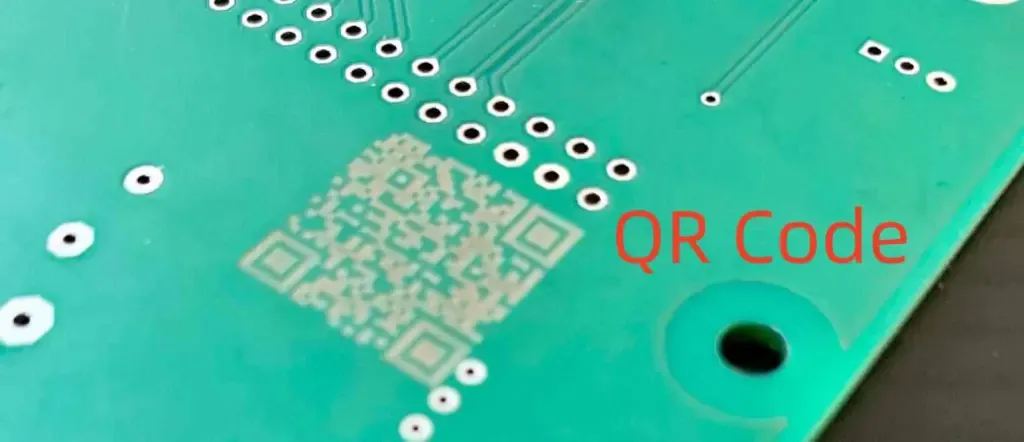
Another exciting development is the use of embedded digital codes, such as DataMatrix or QR codes, etched via laser for traceability. These micro-codes, often smaller than 1 mm2, allow manufacturers to track individual boards through the supply chain, improving quality assurance and recall processes by up to 40% in efficiency.
Conclusion: Elevating High-Density PCB Identification with Advanced Marking
The shift from traditional silkscreen to advanced PCB marking alternatives like direct legend printing and laser marking reflects the growing complexity of high-density boards. These modern techniques address critical component marking challenges, offering superior precision, durability, and efficiency for today’s compact and demanding designs. Whether you prioritize fine resolution for tight spaces or permanent markings for rugged environments, understanding the strengths of each method can transform your PCB manufacturing process.
At ALLPCB, we’re committed to supporting engineers and designers with cutting-edge solutions for high-density PCB identification. By staying ahead of the curve with innovative marking technologies, we help ensure your projects achieve optimal performance and reliability. Explore these advanced techniques in your next design, and see the difference they can make in clarity and quality.