 ALLPCB


Designing printed circuit boards (PCBs) for aerospace applications is no small feat. These boards must perform flawlessly under extreme conditions, from high altitudes to intense vibrations and temperature swings. So, what are the key rules for achieving unwavering reliability in aerospace PCB design? In this blog, we’ll dive into seven essential guidelines that ensure your PCB can withstand the harshest environments while meeting strict industry standards like IPC-A-610 Class 3. Whether you're focused on thermal management, routing strategies, or material selection, these rules will help you build high-reliability PCBs for aerospace projects.
At ALLPCB, we understand the unique challenges of aerospace PCB design. Below, we’ll explore detailed strategies and practical tips to help engineers create boards that meet the rigorous demands of this industry. Let’s get started with the core principles of designing for extreme conditions.
Why Aerospace PCB Design Demands High Reliability
Aerospace environments are among the most challenging for electronic components. PCBs in satellites, aircraft, and spacecraft face temperature extremes ranging from -55°C to 125°C, intense vibrations during launch (up to 20g forces), and radiation exposure in space. A single failure can compromise an entire mission, leading to costly losses or safety risks. This is why aerospace PCB design rules prioritize reliability above all else, adhering to standards like IPC-A-610 Class 3, which demands the highest level of quality for life-critical systems.
High-reliability PCB design isn’t just about meeting standards—it’s about ensuring consistent performance under stress. With this in mind, let’s break down the seven critical rules that guide aerospace PCB design for extreme conditions.
Rule 1: Adhere to IPC-A-610 Class 3 Standards for Quality
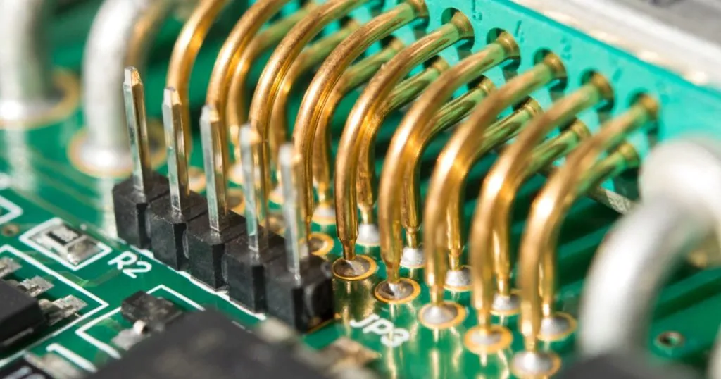
IPC-A-610 Class 3 is the gold standard for high-reliability PCB design, especially in aerospace applications where failure is not an option. This classification sets strict criteria for soldering, component placement, and overall assembly quality. For instance, solder joints must be free of voids and meet precise fillet height requirements to ensure durability under thermal and mechanical stress.
To comply, designers must focus on meticulous documentation and inspection processes. This includes using high-quality materials and ensuring that every via, trace, and component meets the specified tolerances. By following IPC-A-610 Class 3 PCB guidelines, you guarantee that your board can handle the rigors of aerospace environments without cracking or failing.
Rule 2: Prioritize Thermal Management for Extreme Conditions
Aerospace PCB thermal management is critical due to the wide temperature ranges these boards endure. Without proper heat dissipation, components can overheat, leading to performance degradation or failure. For example, a power amplifier in a satellite might generate significant heat, and if not managed, it could exceed its maximum junction temperature of 150°C, causing a shutdown.
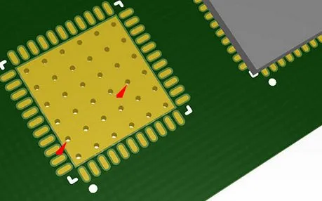
To address this, use materials with high thermal conductivity, such as metal-core PCBs or ceramics, which can handle heat dissipation effectively. Additionally, incorporate thermal vias under heat-generating components to transfer heat to a heat sink or the board’s opposite side. Design layouts with adequate spacing between high-power components to prevent heat buildup, and consider active cooling solutions like fans or heat pipes for critical systems.
Rule 3: Select Materials for Durability in Harsh Environments
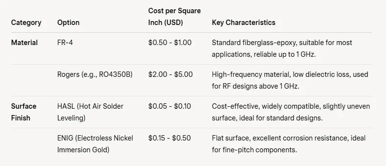
The choice of materials in aerospace PCB design rules can make or break reliability. Standard FR-4 materials often fail under extreme conditions due to their limited thermal and mechanical stability. Instead, opt for high-performance laminates like polyimide or PTFE, which offer excellent resistance to temperature fluctuations and chemical exposure. Polyimide, for instance, can withstand temperatures up to 260°C, making it ideal for aerospace applications.
Beyond the substrate, consider the finish and coating. Conformal coatings protect against moisture, dust, and radiation, while gold plating on connectors ensures corrosion resistance in high-humidity or vacuum environments. These material choices are essential for high-reliability PCB design in extreme conditions.
Rule 4: Optimize Routing for Signal Integrity and Reliability
Aerospace PCB routing guidelines focus on maintaining signal integrity and minimizing interference, especially for high-speed signals used in communication systems. Poor routing can lead to crosstalk, electromagnetic interference (EMI), or signal delays, which are unacceptable in mission-critical applications. For instance, a signal delay of just 1 nanosecond in a radar system could disrupt timing and accuracy.
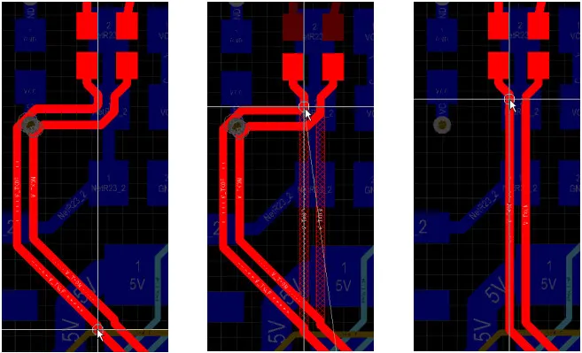
To optimize routing, keep trace lengths as short as possible and maintain consistent impedance—typically 50 ohms for RF signals. Use differential pair routing for high-speed data lines to reduce noise, and separate analog and digital signals to avoid interference. Additionally, avoid sharp 90-degree corners in traces, as they can cause signal reflection; instead, use 45-degree angles or curved traces. Ground planes should be continuous to provide a low-impedance return path and shield against EMI.
Rule 5: Design for Vibration and Mechanical Stress
Aerospace environments subject PCBs to intense mechanical stress, especially during rocket launches or aircraft turbulence. Vibrations can reach frequencies of 20 Hz to 2000 Hz, potentially causing component detachment or trace cracking if the board isn’t designed properly. High-reliability PCB design must account for these forces to prevent failures.
Use thicker boards (e.g., 2.0 mm or more) to increase rigidity, and secure heavy components with additional mounting hardware or adhesives. Place components away from board edges, where stress is highest, and use strain relief for connectors to absorb vibrations. Finite element analysis (FEA) during the design phase can simulate mechanical stress and help identify weak points before manufacturing.
Rule 6: Incorporate Redundancy for Fail-Safe Operation
In aerospace, a single point of failure can be catastrophic. High-reliability PCB design often includes redundancy to ensure continued operation even if a component fails. For example, critical systems like flight control might have duplicate power supplies or backup communication circuits on the same board.
Design redundancy by mirroring essential circuits or using parallel paths for power and signals. However, balance this with space and weight constraints, as aerospace applications prioritize compact, lightweight designs. Test these redundant systems under simulated failure conditions to confirm they activate seamlessly when needed.
Rule 7: Test Rigorously Under Simulated Extreme Conditions
Testing is the final, non-negotiable step in aerospace PCB design. Before deployment, boards must undergo extensive environmental testing to simulate the extreme conditions they’ll face. Thermal cycling tests, for instance, expose the PCB to rapid temperature changes between -55°C and 125°C to check for material expansion or solder joint failure. Vibration tests replicate launch conditions, while radiation testing ensures functionality in space.
Additionally, perform electrical testing for signal integrity and power distribution under load. Use automated optical inspection (AOI) and X-ray imaging to detect hidden defects like micro-cracks or voids in solder joints. Only after passing these rigorous tests can a PCB be deemed ready for aerospace use.
Challenges in Aerospace PCB Design and How to Overcome Them
Designing PCBs for aerospace isn’t without challenges. Miniaturization often conflicts with the need for robust components and redundancy, while cost pressures can limit material choices. Additionally, meeting tight deadlines for mission-critical projects adds stress to the design process.
To overcome these hurdles, leverage advanced design software with built-in simulation tools to predict thermal and mechanical performance early in the process. Collaborate closely with manufacturing teams to ensure design-for-manufacturability (DFM) principles are followed, reducing errors during production. Finally, prioritize iterative testing at each stage to catch issues before they escalate.
The Role of ALLPCB in Aerospace PCB Design
At ALLPCB, we’re committed to supporting engineers in creating high-reliability PCBs for aerospace applications. Our manufacturing processes align with IPC-A-610 Class 3 standards, ensuring top-tier quality for every board. We offer a range of advanced materials and finishes suited for extreme conditions, along with expert guidance on thermal management and routing strategies. With our focus on precision and reliability, we help turn your aerospace PCB designs into reality.
Conclusion: Building Reliability into Every Layer
Aerospace PCB design demands a meticulous approach to achieve unwavering reliability. By following these seven rules—adhering to IPC-A-610 Class 3 standards, prioritizing thermal management, selecting durable materials, optimizing routing, designing for mechanical stress, incorporating redundancy, and testing rigorously—you can create boards that perform flawlessly in the harshest environments. Whether it’s managing heat dissipation or ensuring signal integrity, each step contributes to a PCB that meets the stringent needs of aerospace applications.
With these aerospace PCB design rules in hand, you’re equipped to tackle the challenges of designing for extreme conditions. Focus on precision, test thoroughly, and partner with a trusted manufacturer to bring your high-reliability PCB design to life. At ALLPCB, we’re here to support you every step of the way.





