 ALLPCB


In the world of printed circuit board (PCB) manufacturing, separating individual boards from a larger panel is a critical step. This process, known as depaneling, requires precision to avoid damaging delicate components or compromising board integrity. If you're searching for the best PCB depaneling methods, you're in the right place. This blog explores advanced techniques like laser PCB cutting, PCB routing techniques, and precision PCB sawing, along with the depaneling equipment that makes it all possible. We'll dive deep into each method to help you choose the right solution for your production needs.
What is PCB Depaneling and Why Does It Matter?
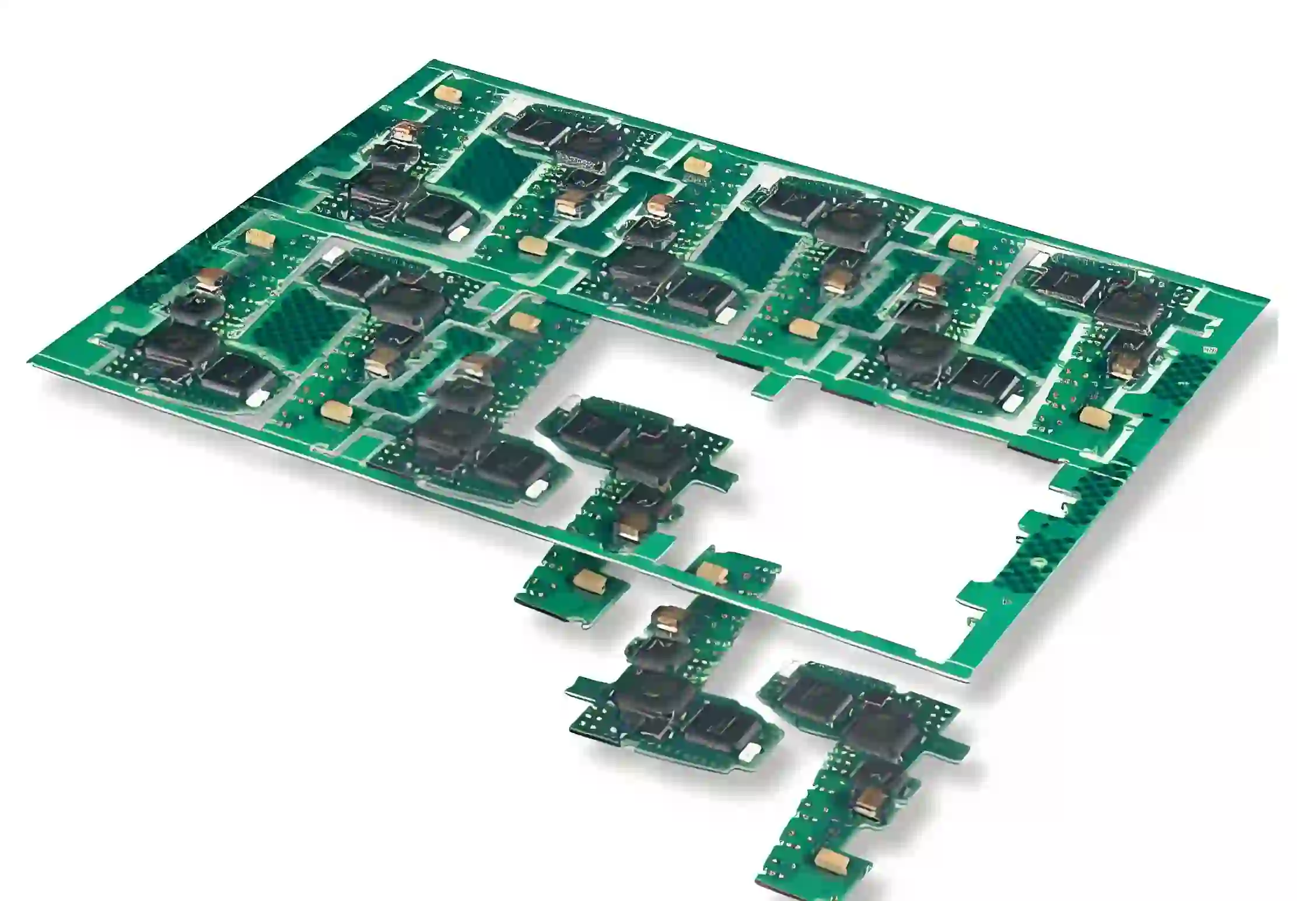
PCB depaneling is the process of separating individual circuit boards from a larger panel after manufacturing. During production, multiple PCBs are often created on a single panel to save time and resources. Once the assembly and testing are complete, these boards must be separated with care to prevent stress, cracks, or damage to components and traces.
Choosing the right depaneling method is crucial because it impacts the quality of the final product, production speed, and overall cost. Poor depaneling can lead to micro-cracks in the board material or damaged solder joints, which might cause failures in the field. With advancements in technology, modern depaneling methods like laser cutting, routing, and precision sawing offer high accuracy and efficiency, catering to different project requirements.
Overview of Advanced PCB Depaneling Methods
Before diving into the specifics, let's briefly outline the three primary advanced depaneling techniques we'll cover. Each method has unique strengths, making it suitable for specific applications in PCB manufacturing.
- Laser PCB Cutting: A non-contact method using focused laser beams to cut through materials with extreme precision, ideal for complex designs and thin boards.
- PCB Routing Techniques: A mechanical process using rotating bits to cut along predefined paths, often used for thicker boards or larger production runs.
- Precision PCB Sawing: A method involving high-speed saw blades to make straight cuts, typically used for simpler designs or high-volume production.
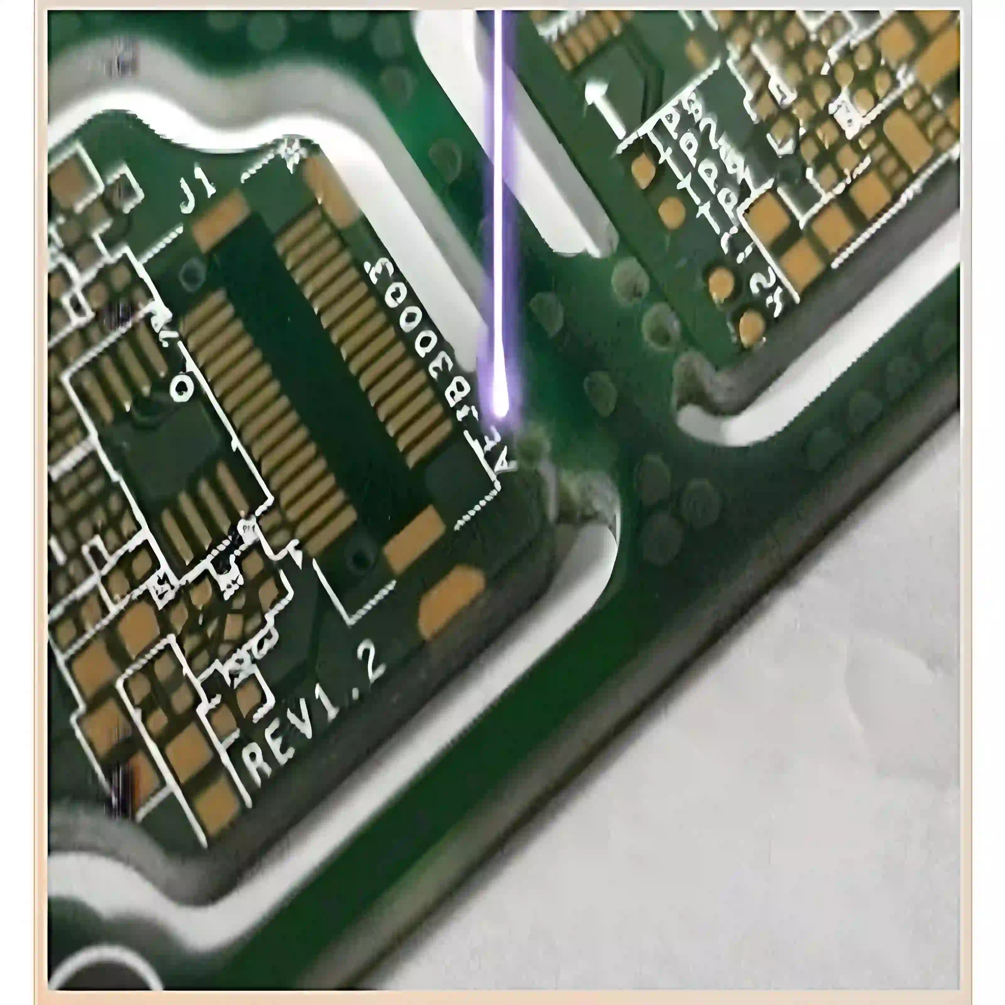
Laser PCB Cutting: Precision Without Contact
Laser PCB cutting has emerged as one of the most advanced PCB depaneling methods due to its unmatched precision and minimal stress on the board. This technique uses a focused laser beam to vaporize material along the cutting line, creating clean edges without physical contact. It's particularly useful for intricate designs, thin substrates, or boards with sensitive components.
How Laser Cutting Works
In laser depaneling, a high-powered laser beam is directed onto the PCB material. The energy from the laser heats and vaporizes the substrate, often a combination of fiberglass and epoxy resin, along with copper traces if present. The process is controlled by computer software, ensuring cuts are made with pinpoint accuracy, sometimes down to tolerances of 0.002 inches (50 micrometers).
Unlike mechanical methods, laser cutting produces no dust or debris since the material is vaporized rather than physically removed. Additionally, there's no tool wear, which reduces maintenance costs over time. However, the process can generate heat, so proper cooling systems or parameter adjustments are necessary to prevent thermal damage to nearby components.
Advantages of Laser PCB Cutting
- High Precision: Capable of cutting intricate shapes and tight tolerances, ideal for densely populated boards.
- No Mechanical Stress: Non-contact cutting eliminates the risk of micro-cracks or component damage.
- Flexibility: Easily adaptable to different board designs through software adjustments.
- Minimal Waste: Vaporization of material means no dust or shavings to clean up.
Limitations of Laser Cutting
- Cost: Initial investment in laser depaneling equipment is higher compared to traditional methods.
- Material Constraints: Not ideal for very thick boards (above 2 mm) as cutting speed decreases significantly.
- Heat Sensitivity: Requires careful control to avoid charring or damaging heat-sensitive components.
PCB Routing Techniques: Mechanical Precision for Versatility
PCB routing is a widely used mechanical depaneling method that involves cutting through the panel using a rotating cutting tool, often referred to as a router bit. This technique is versatile and can handle a variety of materials and PCB board thickness, making it a go-to choice for many manufacturers.
How PCB Routing Works
In PCB routing, a high-speed spindle equipped with a small-diameter router bit (typically 0.8 to 3.0 mm) cuts through the panel along pre-programmed paths. The process is guided by CNC (Computer Numerical Control) systems, ensuring consistent and accurate cuts. Routing is often used for boards with straight or curved separation lines and can handle both scored and unscored panels.
Routing generates dust and debris, so dust extraction systems are essential to maintain a clean working environment and prevent contamination of the boards. The mechanical nature of routing also means that tool wear is a factor, requiring periodic replacement of router bits to maintain cut quality.
Advantages of PCB Routing Techniques
- Versatility: Suitable for a wide range of board thicknesses, from 0.6 mm to over 3.0 mm.
- Cost-Effective: Lower equipment costs compared to laser systems, especially for small to medium production volumes.
- Customizable Cuts: CNC programming allows for complex cutting patterns beyond simple straight lines.
Limitations of Routing
- Mechanical Stress: The physical cutting action can cause vibrations, potentially leading to micro-cracks or stress on components near the cut line.
- Dust Generation: Requires robust dust extraction systems to manage debris.
- Tool Wear: Router bits dull over time, affecting cut quality and requiring regular maintenance.
Precision PCB Sawing: Speed for Straight Cuts
Precision PCB sawing is a mechanical depaneling method that uses high-speed saw blades to make straight cuts through a panel. This technique is often chosen for high-volume production where speed is prioritized over flexibility in cut design. It's best suited for simpler layouts where boards are arranged in a grid pattern.
How Precision Sawing Works
In precision sawing, a circular saw blade, often diamond-coated for durability, rotates at high speeds (up to 60,000 RPM) to slice through the PCB panel. The panel is held securely in a fixture to ensure straight, uniform cuts. Sawing is typically used on panels with V-grooves or score lines, which guide the blade and reduce stress on the material.
Like routing, sawing generates dust and requires effective extraction systems. The method is fast, often completing cuts in seconds per panel, but it lacks the flexibility to handle curved or irregular separation lines.
Advantages of Precision PCB Sawing
- High Speed: Ideal for high-volume production, with cutting times often under 10 seconds per panel.
- Cost Efficiency: Equipment and operational costs are relatively low for large-scale manufacturing.
- Reliability: Produces consistent straight cuts with minimal setup time.
Limitations of Sawing
- Limited Flexibility: Only suitable for straight cuts, not adaptable to complex board shapes.
- Mechanical Stress: Can cause vibrations and stress, risking damage to delicate components.
- Dust and Noise: Generates significant debris and noise, requiring proper safety measures.
Choosing the Right Depaneling Equipment for Your Needs
Selecting the appropriate depaneling equipment depends on several factors, including board design, material thickness, production volume, and budget. Here's a breakdown to help you decide which method aligns with your manufacturing goals.
Factors to Consider
- Board Complexity: For intricate designs or densely populated boards, laser PCB cutting offers the precision needed without risking damage.
- Material Thickness: Thicker boards (above 2 mm) are better suited for PCB routing techniques or precision sawing, as laser cutting becomes less efficient.
- Production Volume: High-volume runs benefit from the speed of precision sawing, while smaller batches or prototypes might justify the investment in laser systems for quality.
- Budget: Mechanical methods like routing and sawing generally have lower upfront costs, while laser systems require a larger initial investment but offer long-term savings on maintenance.
Comparing Depaneling Equipment Costs and Efficiency
To give you a clearer picture, let's compare the approximate costs and efficiency metrics for each method. Note that these figures are general estimates and can vary based on specific equipment models and regional pricing.
- Laser Cutting Equipment: Initial cost ranges from $50,000 to $150,000. Cutting speed is slower for thicker materials (around 10-20 mm/s), but precision is unmatched with tolerances below 0.05 mm.
- Routing Equipment: Costs between $10,000 and $50,000. Cutting speed is moderate (up to 50 mm/s), with tolerances around 0.1 mm, suitable for diverse board types.
- Sawing Equipment: Priced from $5,000 to $30,000. Offers the fastest cutting speed (up to 100 mm/s for straight cuts), but tolerances are wider at approximately 0.2 mm.
Best Practices for Effective PCB Depaneling
Regardless of the method you choose, following best practices ensures optimal results and minimizes the risk of damage to your PCBs. Here are some actionable tips for successful depaneling.
- Design for Depaneling: Incorporate V-grooves or score lines in your panel design to guide cuts and reduce stress, especially for mechanical methods like sawing and routing.
- Use Proper Fixturing: Secure the panel firmly during depaneling to prevent movement, which can lead to inaccurate cuts or damage.
- Optimize Parameters: For laser cutting, adjust power and speed settings to match the material thickness and avoid thermal damage. For mechanical methods, ensure tools are sharp and dust extraction is active.
- Regular Maintenance: Keep equipment in top condition by replacing worn router bits or saw blades and calibrating laser systems for consistent performance.
- Quality Inspection: After depaneling, inspect boards for micro-cracks, burrs, or thermal damage using magnification tools or automated optical inspection systems.
Suggested Reading: Optimizing PCB Depaneling: A Comprehensive Guide to Methods and Best Practices
Future Trends in PCB Depaneling Technology
As technology evolves, so do PCB depaneling methods. Innovations are focused on increasing precision, reducing costs, and enhancing sustainability. For instance, advancements in laser technology are leading to faster cutting speeds and the ability to handle thicker materials without thermal impact. Additionally, automation and AI integration in depaneling equipment are streamlining processes, allowing for real-time adjustments and error detection during production.
Another trend is the push toward eco-friendly manufacturing. Newer systems aim to minimize energy consumption and waste, with laser cutting leading the way due to its lack of physical debris. Staying updated on these trends can help manufacturers remain competitive and meet evolving industry standards.
Suggested Reading: The Future of PCB Depaneling: Emerging Trends and Technologies
Conclusion: Making the Right Choice for PCB Depaneling
PCB depaneling is a vital step in manufacturing that demands careful consideration of method and equipment. Laser PCB cutting offers unmatched precision for complex, delicate boards, while PCB routing techniques provide versatility for a range of materials and designs. Precision PCB sawing stands out for its speed and cost-effectiveness in high-volume, straightforward applications. By understanding the strengths and limitations of each method, along with your specific production needs, you can select the best depaneling approach to ensure quality and efficiency.
Investing in the right depaneling equipment and following best practices can significantly enhance your manufacturing process, leading to reliable, high-quality circuit boards. Whether you're working on prototypes or large-scale production, these advanced techniques provide the tools to achieve flawless results every time.


