 ALLPCB


Navigation systems are at the heart of modern technology, guiding everything from vehicles to drones with precision and reliability. The core of these systems lies in the Printed Circuit Board (PCB) assembly, a complex process that demands accuracy and expertise. If you're looking for insights into navigation PCB assembly, you've come to the right place. This guide will walk you through the essential techniques and processes, including navigation PCB SMT assembly, navigation PCB through-hole assembly, navigation PCB soldering techniques, navigation PCB component placement, and navigation PCB reflow profiling. Whether you're an engineer or a manufacturer, this detailed resource will help you understand and optimize the assembly process for navigation systems.
Why Navigation System PCB Assembly Matters
Navigation systems rely on PCBs to process signals, manage data, and ensure seamless communication between components like GPS modules, sensors, and microcontrollers. A well-assembled PCB is critical for achieving high performance, minimizing signal interference, and ensuring durability in harsh environments. For instance, automotive navigation systems must withstand temperature fluctuations and vibrations, which means the PCB assembly must be robust and precise.
In this guide, we'll break down each step of the assembly process, focusing on the unique challenges and best practices for navigation systems. Let's dive into the key techniques that ensure a reliable and efficient PCB for navigation applications.
Understanding Navigation PCB SMT Assembly
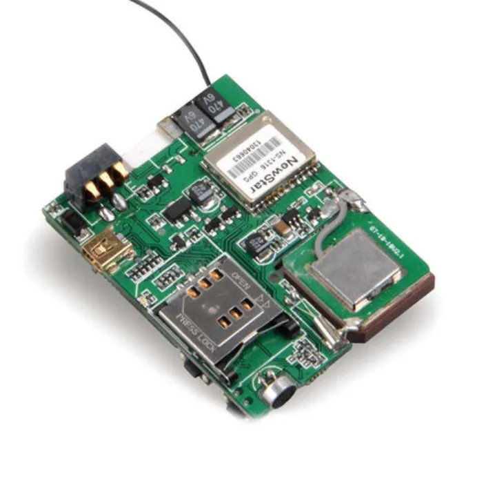
Surface Mount Technology (SMT) is the go-to method for assembling modern navigation PCBs due to its ability to place small, high-density components directly onto the board's surface. Navigation PCB SMT assembly is ideal for compact designs, which are common in GPS devices and wearable navigation tools where space is limited.
The SMT assembly process for navigation PCBs involves several key steps:
- Solder Paste Application: A stencil is used to apply solder paste to specific areas of the PCB where components will be placed. Precision is crucial here to avoid excess paste, which can cause short circuits in the tight layouts of navigation systems.
- Component Placement: Automated pick-and-place machines position tiny components like resistors, capacitors, and integrated circuits onto the solder paste. For navigation PCBs, components such as GPS receivers must be placed with exact alignment to ensure signal integrity, often within tolerances of 0.1mm.
- Reflow Soldering: The PCB passes through a reflow oven where the solder paste melts and forms a permanent bond between components and the board. Temperature profiles are carefully controlled to prevent thermal stress on sensitive navigation components.
One challenge in navigation PCB SMT assembly is managing high-frequency signals. GPS modules operate at frequencies around 1.575 GHz, so any misalignment or poor soldering can lead to signal loss. Using advanced inspection tools like Automated Optical Inspection (AOI) ensures that components are correctly placed and soldered.
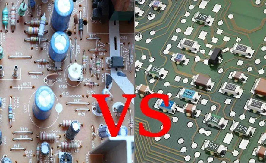
Exploring Navigation PCB Through-Hole Assembly
While SMT dominates modern PCB assembly, navigation PCB through-hole assembly still plays a vital role, especially for components that require extra mechanical strength. Through-hole technology (THT) involves inserting component leads into drilled holes on the PCB and soldering them on the opposite side. This method is often used for larger components in navigation systems, such as power connectors or antennas, which need to endure physical stress.
The through-hole assembly process includes:
- Component Insertion: Components are manually or automatically inserted into pre-drilled holes. For navigation systems, connectors for external antennas might be mounted this way to ensure a stable connection.
- Soldering: Wave soldering is commonly used, where the PCB passes over a wave of molten solder to secure the leads. This creates a strong bond, critical for components exposed to vibration in automotive or marine navigation devices.
- Inspection: After soldering, the board is inspected for issues like cold solder joints, which could lead to unreliable connections in navigation systems.
Navigation PCB through-hole assembly is less common in compact designs but remains essential for hybrid boards where both SMT and THT are used. For example, a navigation system might use SMT for microcontrollers and THT for power input connectors to balance compactness with durability.
Mastering Navigation PCB Soldering Techniques
Soldering is the backbone of any PCB assembly, and navigation PCB soldering techniques must be tailored to meet the high reliability standards of these systems. Poor soldering can result in signal interference or component failure, which is unacceptable in applications where accuracy is paramount.
Here are the primary soldering techniques used in navigation PCB assembly:
- Reflow Soldering for SMT: As mentioned earlier, reflow soldering is used for surface-mount components. The process involves heating the PCB in a controlled oven to melt the solder paste. For navigation systems, the reflow profile must avoid overheating sensitive components like GPS chips, which can degrade if exposed to temperatures above 260°C for too long.
- Wave Soldering for THT: This technique is used for through-hole components, passing the PCB over a wave of molten solder. It's efficient for high-volume production but requires careful control to prevent solder bridges in densely packed navigation boards.
- Hand Soldering: For rework or small-batch production, hand soldering is sometimes used. This technique demands skilled technicians to avoid damaging delicate navigation components, especially when replacing a faulty sensor or connector.
A key consideration in navigation PCB soldering techniques is the choice of solder material. Lead-free solder, compliant with RoHS standards, is often used, but it requires higher melting temperatures (around 217-220°C) compared to traditional lead-based solder. This can stress components if not managed properly, so precise temperature control is essential.
Optimizing Navigation PCB Component Placement
Effective navigation PCB component placement is critical for ensuring signal integrity, thermal management, and overall system performance. Navigation systems often handle high-frequency signals and sensitive data, so the layout and placement of components must minimize interference and crosstalk.
Here are some best practices for navigation PCB component placement:
- Group Related Components: Place components like GPS receivers, oscillators, and RF amplifiers close together to reduce signal path length. For example, keeping the GPS antenna input near the receiver chip minimizes signal loss at 1.575 GHz.
- Avoid Noise Sources: Position sensitive components away from power supplies or high-current traces that could introduce electromagnetic interference (EMI). This is especially important for navigation systems, where even minor noise can disrupt GPS accuracy.
- Thermal Considerations: Place heat-generating components, such as voltage regulators, in areas with good airflow or near heat sinks. Overheating can affect the performance of navigation chips, which often operate best below 85°C.
- Use Automated Tools: Modern pick-and-place machines ensure precision within 0.05mm, which is vital for densely packed navigation PCBs where space is at a premium.
Additionally, designers must consider the board's layer stack-up. For navigation systems, a multilayer PCB with dedicated ground planes can shield sensitive signals from interference, ensuring reliable operation even in noisy environments.
Perfecting Navigation PCB Reflow Profiling
Reflow profiling is a critical step in navigation PCB assembly, especially for SMT components. Navigation PCB reflow profiling involves setting the correct temperature curve in the reflow oven to ensure proper soldering without damaging components. A poorly designed profile can lead to issues like tombstoning, where components lift off the board, or insufficient solder joints that fail under stress.
The reflow process typically follows four stages:
- Preheat: The PCB is gradually heated to around 150-180°C to activate the flux in the solder paste and prevent thermal shock. For navigation PCBs, a slow ramp-up rate of 1-2°C per second is ideal to protect sensitive components.
- Soak: The board is held at a steady temperature (around 180-200°C) to ensure even heating. This stage, lasting 60-90 seconds, helps remove moisture and prepares the solder for melting.
- Reflow: The temperature peaks at 235-250°C for a short duration (20-40 seconds) to melt the solder and form strong joints. For navigation systems, staying within the component’s thermal limits is crucial—many GPS chips have a maximum tolerance of 260°C.
- Cooling: The PCB cools down at a controlled rate of 2-4°C per second to solidify the solder joints without causing thermal stress or cracking.
Creating an effective reflow profile for navigation PCBs requires testing and adjustment. Using a thermal profiler to monitor temperatures across the board ensures consistency, especially for complex designs with varying component sizes. A well-executed reflow profile reduces defects and enhances the reliability of navigation systems in real-world conditions.
Challenges in Navigation System PCB Assembly
Assembling PCBs for navigation systems comes with unique challenges that require specialized solutions:
- High-Frequency Signal Integrity: Navigation systems operate at frequencies like 1.575 GHz for GPS signals. Any impedance mismatch or poor soldering can degrade performance. Designers must use controlled impedance traces (typically 50 ohms) and precise soldering techniques to maintain signal quality.
- Environmental Durability: Navigation devices in vehicles or outdoor equipment face extreme conditions, from -40°C to 85°C. PCBs must be assembled with materials and techniques that resist thermal expansion and vibration.
- Miniaturization: As navigation systems become smaller, fitting high-performance components into tight spaces is a challenge. Advanced SMT assembly with micro-components (down to 0201 sizes) is often necessary.
Addressing these challenges requires collaboration between designers, engineers, and assembly teams to ensure every aspect of the PCB meets the stringent demands of navigation applications.
Best Practices for Quality Assurance in Navigation PCB Assembly
Quality assurance (QA) is non-negotiable in navigation PCB assembly. A single defect can compromise the entire system, leading to inaccurate positioning or complete failure. Here are some best practices to ensure high-quality assembly:
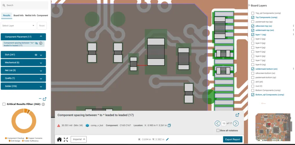
- Automated Inspection: Use AOI and X-ray inspection to detect soldering defects, misaligned components, or hidden issues like voids in solder joints.
- Functional Testing: Test the PCB under real-world conditions to verify GPS signal reception, data processing, and power management. For example, simulate temperature cycles between -20°C and 70°C to ensure reliability.
- Traceability: Implement systems to track components and assembly processes. This helps identify the root cause of any issues and ensures compliance with industry standards like IPC-A-610 for electronics assembly.
By prioritizing QA, manufacturers can deliver navigation PCBs that meet the high standards required for critical applications.
Conclusion: Building Reliable Navigation Systems with Expert PCB Assembly
Navigation system PCB assembly is a complex but rewarding process that demands precision, expertise, and attention to detail. From navigation PCB SMT assembly and through-hole techniques to soldering, component placement, and reflow profiling, each step plays a vital role in creating a reliable and high-performing board. By following the best practices outlined in this guide, you can optimize your assembly process to meet the unique challenges of navigation systems, ensuring accuracy and durability in every application.
Whether you're designing a PCB for automotive GPS, marine navigation, or wearable devices, understanding these techniques will help you achieve superior results. With the right approach to navigation PCB assembly, you can build systems that guide the way with confidence and precision.


