 ALLPCB


Printed Circuit Boards (PCBs) are the backbone of modern electronics, connecting components to create functional devices. However, even experienced engineers can make mistakes during the PCB design process that lead to costly delays, unreliable performance, or manufacturing challenges. In this blog, we explore seven common PCB design mistakes and provide practical tips to avoid them, ensuring your designs are robust, efficient, and manufacturable. Whether you're designing a high-speed board for a server or a compact circuit for a wearable device, these insights will help you achieve better results.
1. Incorrect Component Footprints
The Mistake
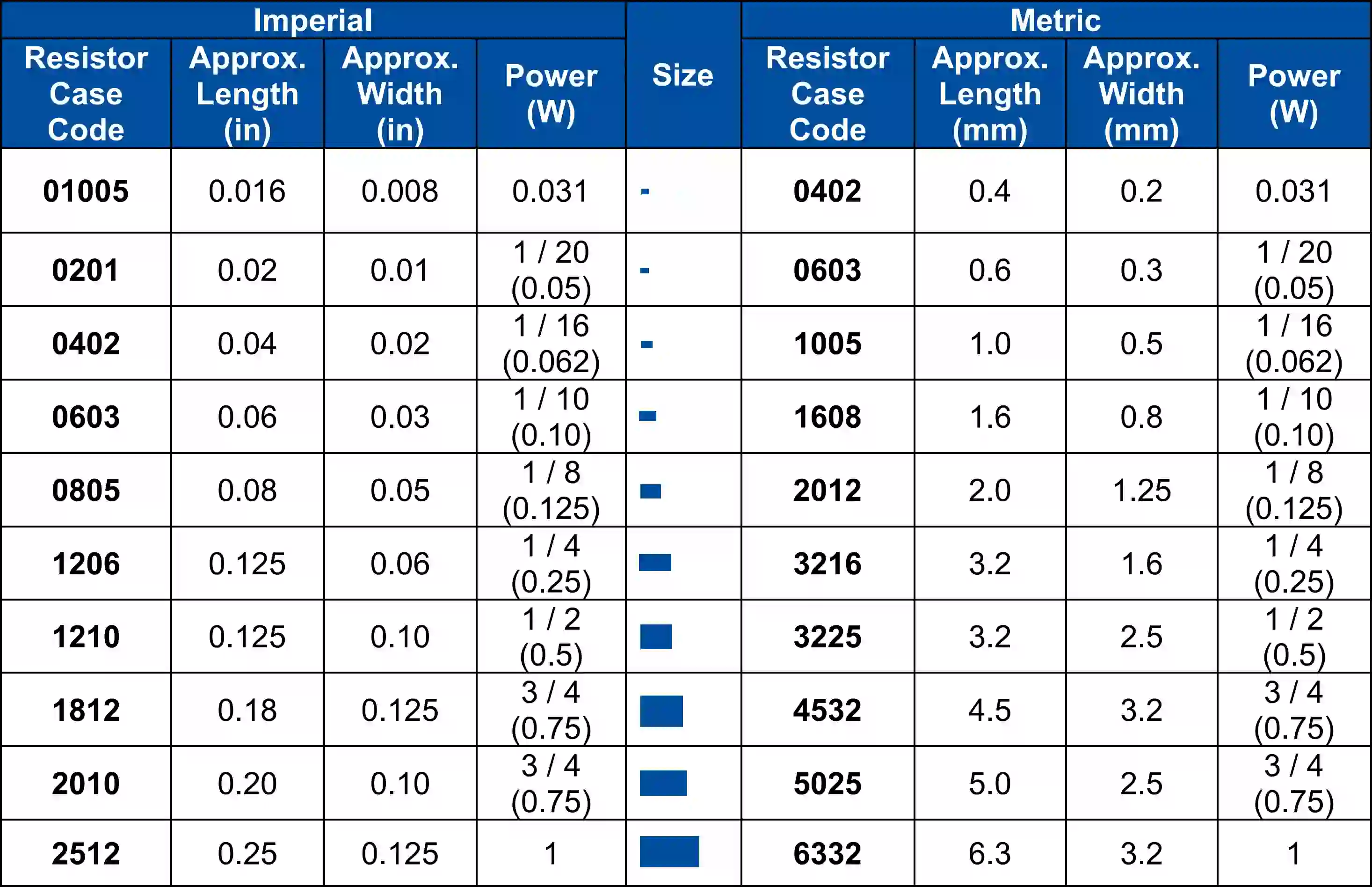
One of the most frequent PCB design errors is using incorrect component footprints. A footprint defines the physical layout of a component on the PCB, including pad sizes, shapes, and spacing. Using a footprint that doesn't match the component's specifications can lead to assembly issues, such as misaligned components or poor solder joints. For example, a designer might select a footprint from a software library assuming it matches a specific capacitor, only to find during prototyping that the pad sizes are too small, causing soldering failures.
How to Avoid It
- Verify Footprint Data: Always cross-check the component's datasheet against the footprint in your design software. For instance, a 0805 resistor typically requires pads of approximately 1.2 mm x 1.0 mm, but slight variations in manufacturer specifications can affect compatibility.
- Use Manufacturer-Recommended Footprints: Component manufacturers often provide recommended footprints in their datasheets. Stick to these whenever possible to avoid mismatches.
- Conduct a Design Review: Have a colleague or third-party engineer review your schematic and layout to catch footprint errors before manufacturing.
2. Inadequate Trace Width and Spacing
The Mistake
Trace width and spacing are critical for ensuring signal integrity and preventing electrical issues like short circuits or crosstalk. A common mistake is using traces that are too narrow for the current they carry or spacing traces too closely, leading to overheating or signal interference. For example, a trace carrying 1A of current on a 1 oz copper layer needs to be at least 0.5 mm wide to avoid excessive heat buildup, but inexperienced designers might use a narrower 0.2 mm trace, risking failure.
How to Avoid It
- Calculate Trace Width: Use a trace width calculator to determine the appropriate width based on current, copper thickness, and temperature rise. For instance, for a 1A current on a 1 oz copper PCB, a trace width of 0.5 mm allows a temperature rise of less than 10°C.
- Follow IPC Standards: Adhere to IPC-2221 guidelines for minimum trace spacing to prevent flashovers. For a 50V circuit, maintain at least 0.6 mm spacing between traces to avoid arcing.
- Simulate High-Speed Signals: For high-speed designs, use simulation tools like SPICE to analyze signal integrity and ensure trace spacing minimizes crosstalk.
3. Poor Component Placement
The Mistake
Improper component placement can lead to signal integrity issues, thermal problems, or assembly difficulties. For example, placing high-speed components like microcontrollers far apart increases trace lengths, which can degrade signal quality at frequencies above 100 MHz. Similarly, placing heat-generating components like power regulators too close together can cause overheating, reducing the PCB's lifespan.
How to Avoid It
- Group Related Components: Place components with functional relationships (e.g., a microcontroller and its decoupling capacitors) close together to minimize trace lengths. Decoupling capacitors should be within 5 mm of the power pin they serve.
- Consider Thermal Management: Space out heat-generating components and place them near thermal vias or heat sinks. For example, a power MOSFET generating 5W of heat requires at least 10 mm² of thermal via area to dissipate heat effectively.
- Use Auto-Placement Tools: Modern CAD software offers auto-placement features to optimize component layout, but always review the results manually to ensure practicality.
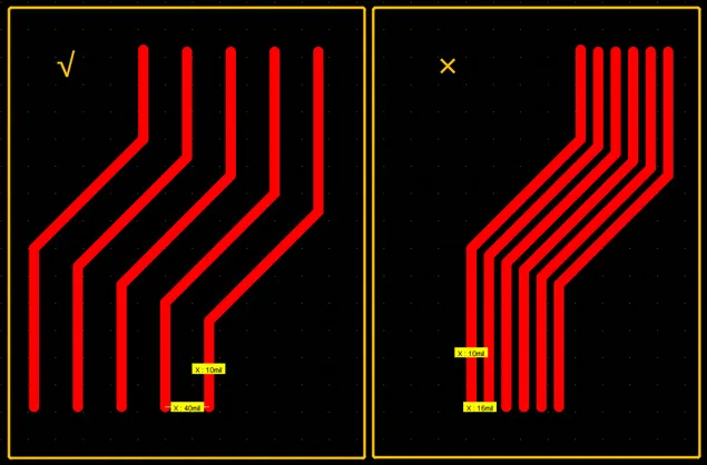
4. Neglecting Signal Integrity
The Mistake
Signal integrity issues, such as noise, reflections, or electromagnetic interference (EMI), often arise from poor routing practices or inadequate grounding. For instance, in high-speed designs operating at 1 GHz, mismatched impedance in a 50-ohm transmission line can cause signal reflections, reducing data reliability. Neglecting ground planes or using inconsistent trace widths can exacerbate these problems.
How to Avoid It
- Maintain Impedance Control: Use an impedance calculator to set trace widths for controlled impedance lines. For a 50-ohm microstrip on a 1.6 mm FR4 board, a trace width of approximately 0.3 mm is typical.
- Implement Robust Ground Planes: Use continuous ground planes to provide a low-impedance return path for signals. Avoid splitting ground planes unless necessary for analog-digital separation.
- Route High-Speed Signals Carefully: Keep high-speed traces short and straight, avoiding 90° angles to reduce EMI. For differential pairs, ensure traces are equal in length to within 0.1 mm to prevent signal skew.
5. Inadequate Power Distribution
The Mistake
A poorly designed power distribution network can lead to voltage drops, noise, or unstable operation. A common error is placing decoupling capacitors too far from power pins, reducing their effectiveness. For example, a capacitor placed 20 mm away from a microcontroller's power pin may fail to filter high-frequency noise above 100 MHz, causing erratic behavior.
How to Avoid It
- Place Decoupling Capacitors Close to Pins: Position capacitors within 5 mm of the power pin they serve, ideally with a direct connection to the power plane.
- Use Multiple Capacitors: Combine capacitors of different values (e.g., 0.1 µF and 10 µF) to filter a wide range of frequencies.
- Design Wide Power Traces: For high-current paths, use wider traces or power planes to minimize resistance. A 1 oz copper trace carrying 3A should be at least 1.5 mm wide to limit voltage drop.
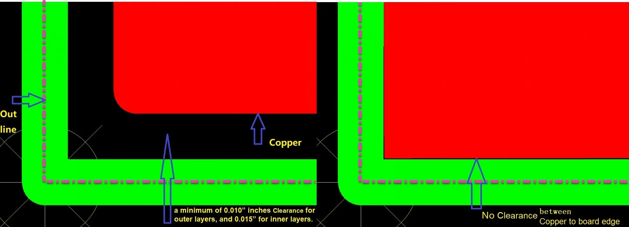
6. Ignoring Design for Manufacturability (DFM)
The Mistake
Failing to consider manufacturing constraints can lead to costly rework or production delays. Common DFM errors include insufficient copper-to-edge clearance (e.g., less than 0.5 mm), which risks exposing copper during depanelization, or using vias too close to component pads, causing solder bridges. These issues can increase manufacturing costs by up to 20% due to rework.
How to Avoid It
- Follow DFM Guidelines: Consult your manufacturer's DFM checklist early in the design process. For example, maintain at least 0.5 mm clearance between copper and board edges to prevent burrs.
- Perform DFM Checks: Use CAD software with built-in DFM analysis to identify issues like insufficient annular rings or solder mask clearance before production.
- Collaborate with Manufacturers: Engage with your PCB fabricator early to align your design with their capabilities, such as minimum drill sizes (e.g., 0.2 mm for standard vias).
7. Skipping Design Reviews and Testing
The Mistake
Rushing to production without thorough design reviews or testing is a recipe for failure. Even experienced designers can overlook issues like hairline short circuits or incorrect via types (e.g., using blind vias when unnecessary, increasing costs by 30-50%). Prototypes may work initially but fail under real-world conditions due to untested environmental factors like temperature or vibration.
How to Avoid It
- Conduct Peer Reviews: Have multiple engineers review your schematic and layout to catch errors. A second set of eyes can spot issues like incorrect via placements that you might miss.
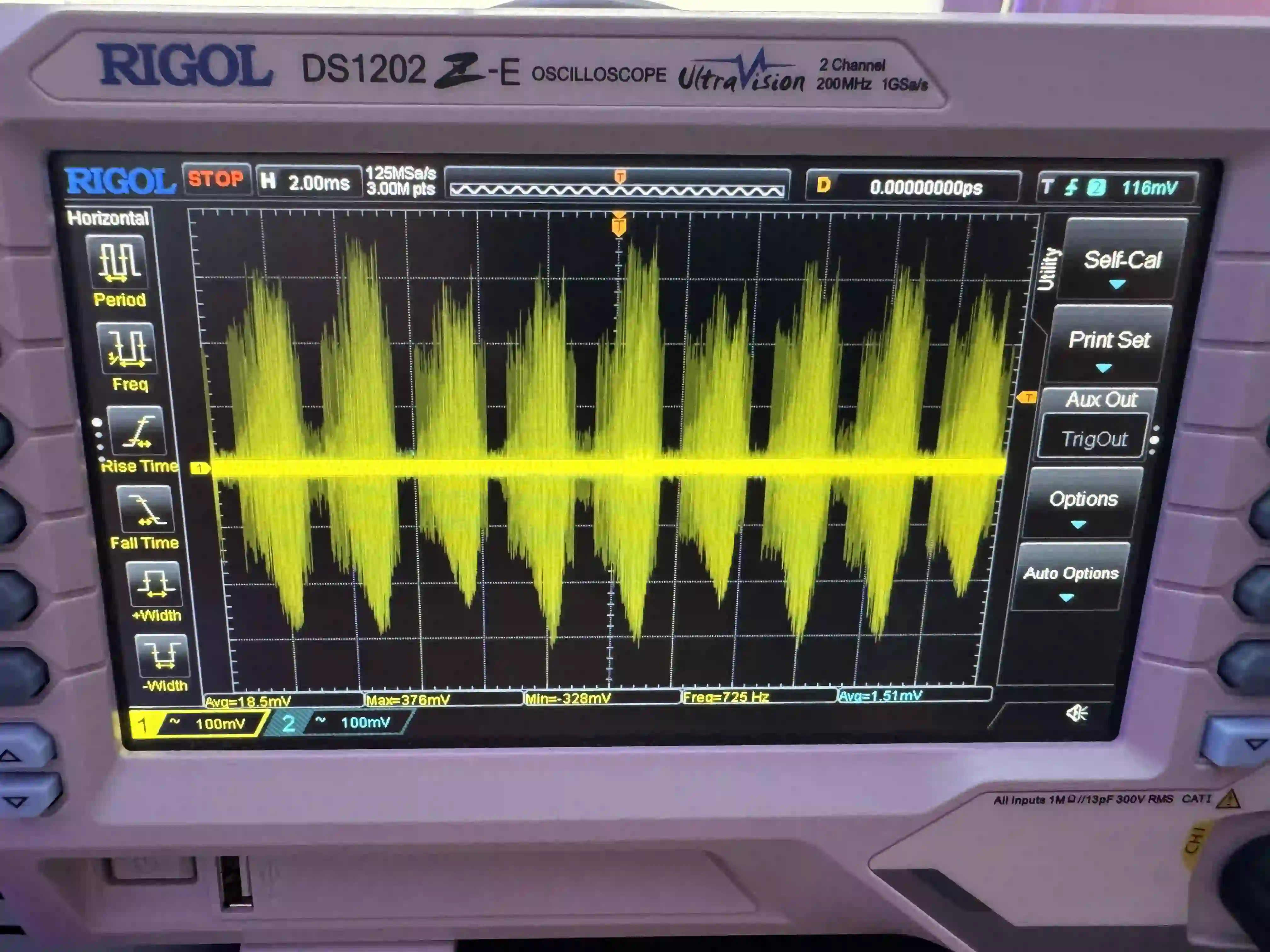
- Test Prototypes Thoroughly: Use tools like multimeters, oscilloscopes, and signal analyzers to verify functionality. For example, test high-speed signals at 1 GHz to ensure no reflections occur.
- Simulate Environmental Conditions: Subject prototypes to thermal cycling (e.g., -40°C to 85°C) and vibration tests to ensure reliability in the intended application.
How ALLPCB Supports Your PCB Design Success
At ALLPCB, we understand the challenges of designing reliable, high-performance PCBs. Our quick-turn prototyping services allow you to test and refine your designs rapidly, reducing time-to-market. With advanced manufacturing capabilities, we support complex designs with tight tolerances, such as 0.1 mm trace widths and 0.2 mm vias, ensuring your boards meet stringent quality standards. Our global logistics network ensures fast delivery, while our expert team provides DFM feedback to help you avoid common pitfalls like those discussed above. By partnering with ALLPCB, you can confidently bring your designs to life with precision and efficiency.
Conclusion
Designing a PCB is a complex process that requires attention to detail and adherence to best practices. By avoiding these seven common mistakes—incorrect footprints, inadequate trace widths, poor component placement, neglecting signal integrity, inadequate power distribution, ignoring DFM, and skipping reviews—you can create reliable, manufacturable boards that perform as intended. Incorporate simulation tools, follow industry standards like IPC-2221, and collaborate with your manufacturer to catch errors early. With these strategies, you'll save time, reduce costs, and deliver high-quality electronics that meet your project goals.


