ALLPCB


If you're looking to achieve clean and efficient PCB separation, mastering tab routing and breakaway tabs is essential. In this comprehensive guide, we'll dive into the art of PCB tab routing design, explore the role of mouse bites PCB techniques, and share tips to enhance breakaway tab strength. You'll also learn proven PCB depaneling methods and clean separation techniques to ensure high-quality results in your manufacturing process. Whether you're a beginner or a seasoned engineer, this masterclass will equip you with actionable insights to optimize your PCB panelization.
What Are Breakaway Tabs and Why Do They Matter?
Breakaway tabs, often referred to as mouse bites PCB features, are small perforated or scored connections used in PCB panelization. These tabs hold multiple circuit boards together during manufacturing and assembly, allowing them to be easily separated afterward. Their primary purpose is to ensure stability during production while enabling clean separation techniques without damaging the individual boards.
The design and strength of these tabs directly impact the quality of the final product. Poorly designed tabs can lead to jagged edges, stress fractures, or even damage to critical components near the board's edge. On the other hand, well-optimized breakaway tab strength ensures smooth separation and minimizes remnant material, saving time and reducing costs. In the following sections, we'll break down the key elements of PCB tab routing design and provide practical strategies for success.
Understanding PCB Tab Routing Design Basics
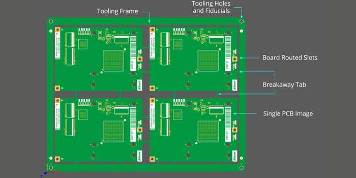
PCB tab routing design is the process of creating pathways or outlines on a panel to define where individual boards will be separated. Tab routing involves strategically placing breakaway tabs along these outlines to hold the boards in place during fabrication. Unlike V-scoring, which uses a continuous cut line, tab routing relies on small, intermittent tabs that can be snapped apart manually or with minimal tools.
The goal of tab routing is to balance stability and ease of separation. If the tabs are too strong, breaking them apart can cause stress on the board, leading to cracks or delamination. If they’re too weak, the panel may break prematurely during handling or assembly. A typical tab width ranges from 0.2 mm to 0.5 mm, depending on the board thickness (commonly 1.6 mm for standard PCBs) and material (like FR-4). Adjusting the number of tabs—often 3 to 5 per side—also plays a role in achieving the right balance.
Designing effective tabs requires attention to the board's edge clearance. Ensure that no components or traces are placed within 2-3 mm of the tab area to prevent damage during separation. This clearance also allows for smoother post-separation cleanup, reducing the need for sanding or additional finishing.
The Role of Mouse Bites in PCB Depaneling
Mouse bites PCB design is a specific type of breakaway tab technique that uses small, perforated holes to create a weak connection point. These perforations resemble tiny bite marks—hence the name—and are typically arranged in a line with hole diameters of 0.5 mm to 1.0 mm, spaced 1.0 mm apart. Mouse bites are a popular choice for PCB depaneling because they allow for clean, tool-free separation while maintaining enough strength to hold the panel together during production.
One key advantage of mouse bites is their ability to minimize stress on the board. The perforations distribute force evenly during separation, reducing the risk of cracks compared to solid tabs. However, the placement and number of holes must be carefully calculated. For a standard 1.6 mm thick FR-4 board, using 5 to 7 holes per tab often provides optimal results. Too few holes can make the tab too strong, while too many can weaken it excessively.
Optimizing Breakaway Tab Strength for Durability and Ease
Achieving the right breakaway tab strength is a critical aspect of tab routing design. The strength of a tab depends on several factors, including its width, thickness, material, and the number of connection points. For most standard PCBs, a tab width of 0.3 mm to 0.5 mm offers a good balance between holding power and ease of separation. Thicker boards (e.g., 2.0 mm or more) may require slightly wider tabs to maintain stability.
The material of the PCB also influences tab strength. FR-4, a common PCB substrate, has a tensile strength of approximately 310 MPa, which provides good durability for breakaway tabs. However, if you're working with more brittle materials like ceramics, you may need to reduce tab width or increase the number of mouse bite holes to prevent cracking during separation.
Another factor to consider is the tab's location. Place tabs away from high-stress areas or corners of the board, as these spots are more prone to damage. Distributing tabs evenly along the board's edge—typically one every 50-75 mm—ensures uniform stress distribution. For added precision, some designers use simulation software to predict stress points and adjust tab placement accordingly.
Best Practices for PCB Depaneling with Clean Separation Techniques
PCB depaneling is the process of separating individual boards from a panel after assembly. Using effective clean separation techniques during depaneling is crucial to avoid damaging the boards or leaving rough edges that require additional processing. Below are some best practices to ensure smooth and precise separation:
- Manual Separation with Mouse Bites: For panels with mouse bites, manual separation is often sufficient. Gently flex the panel at the tab locations to break the connections. Use gloves to avoid injury from sharp edges, and ensure the force is applied evenly to prevent uneven breaks.
- Tool-Assisted Depaneling: For stronger tabs or larger panels, a depaneling tool like a pizza cutter-style roller or a guillotine cutter can provide cleaner results. These tools apply consistent pressure along the tab line, minimizing stress on the board. Ensure the tool's blade aligns precisely with the tab routing path.
- Post-Separation Cleanup: After separation, inspect the board edges for burrs or remnants. A fine-grit sandpaper (e.g., 400-600 grit) can smooth out rough spots without damaging the board. Alternatively, some manufacturers use automated edge-finishing machines for high-volume production.
Regardless of the method, always prioritize safety and precision. Rushing the depaneling process can lead to damaged traces or components, especially if they’re placed too close to the board edge. Maintaining a clearance of at least 2 mm between components and the separation line is a good rule of thumb.
Common Challenges in Tab Routing and How to Overcome Them
Even with careful planning, challenges can arise in PCB tab routing design and depaneling. Here are some common issues and solutions to help you achieve optimal results:
- Cracking or Delamination: This often occurs when tabs are too strong or when force is applied unevenly during separation. To prevent this, reduce tab width or increase the number of mouse bite holes. Additionally, ensure that the panel is supported evenly during depaneling to avoid localized stress.
- Rough Edges After Separation: Rough edges are a sign of poorly designed tabs or improper separation techniques. Using mouse bites with a consistent hole pattern (e.g., 0.8 mm diameter holes spaced 1.2 mm apart) can minimize this issue. Post-separation sanding or edge finishing can also help.
- Premature Breakage: If tabs break during assembly or handling, they may be too weak. Increase tab width slightly (e.g., from 0.3 mm to 0.4 mm) or reduce the number of perforations in mouse bites. Testing a prototype panel before full production can help identify and address this problem early.
By anticipating these challenges and adjusting your design accordingly, you can save time and resources while ensuring high-quality PCB separation.
Advanced Tips for Optimizing Breakaway Tabs
For engineers looking to take their breakaway tab strength and tab routing to the next level, consider these advanced strategies:
- Use Simulation Tools: Software tools can model stress distribution during separation, helping you fine-tune tab placement and width. These simulations can predict potential failure points and guide adjustments before manufacturing.
- Experiment with Hybrid Designs: Combine mouse bites with solid tabs in areas that require extra strength. For example, use solid tabs near corners for added stability and mouse bites along straight edges for easier separation.
- Customize Based on Board Size: Larger boards (e.g., over 200 mm in length) may require more tabs to prevent flexing during handling. A general guideline is to add one tab for every 50 mm of edge length, adjusting based on the board's weight and material.
These advanced techniques require additional planning but can significantly improve the efficiency and quality of your PCB panelization process.
Conclusion: Mastering PCB Tab Routing for Superior Results
Optimizing PCB tab routing design and breakaway tabs is a critical skill for achieving clean and efficient PCB separation. By understanding the role of mouse bites PCB techniques, fine-tuning breakaway tab strength, and applying proven PCB depaneling methods, you can ensure high-quality results in your manufacturing process. The clean separation techniques discussed in this guide—such as proper tab placement, balanced strength, and careful depaneling—will help you minimize damage, reduce waste, and streamline production.
Whether you're designing a small prototype or managing high-volume production, the principles of tab routing remain the same: balance stability with ease of separation, prioritize edge clearance, and test your designs before scaling up. With these strategies in hand, you're well on your way to mastering the art of PCB panelization and delivering flawless boards every time.