ALLPCB


Designing printed circuit boards (PCBs) for radio frequency (RF) applications is a complex task that demands precision and specialized tools. If you're searching for the right RF PCB design software, you likely need features that support high-frequency PCB layout, impedance matching tools, signal integrity for RF, and PCB design for wireless communication. In short, the essential features of RF PCB design software include advanced simulation tools, precise impedance control, robust signal integrity analysis, and support for high-frequency materials and layouts.
In this comprehensive guide, we'll dive deep into these critical features, explaining why they matter and how they help engineers create reliable, high-performance RF PCBs. Whether you're working on wireless communication systems or high-frequency circuits, this blog will help you understand what to look for in design software to meet your project needs.
Why RF PCB Design Requires Specialized Software
RF PCB design is different from standard PCB design due to the unique challenges of high-frequency signals. At frequencies above a few megahertz, issues like signal loss, crosstalk, and electromagnetic interference (EMI) become significant. Standard PCB design tools often lack the capabilities to handle these challenges, making specialized RF PCB design software a necessity.
For example, high-frequency signals can behave unpredictably if traces aren't designed with precise impedance control. A mismatch in impedance can cause signal reflections, leading to data loss or system failure. RF design software addresses these issues with tools tailored for high-frequency PCB layout and signal integrity for RF, ensuring your designs perform as intended.
Key Features to Look for in RF PCB Design Software
Choosing the right software for RF applications means focusing on features that address the specific needs of high-frequency design. Below, we break down the essential tools and capabilities that make a difference in RF PCB projects.
1. High-Frequency PCB Layout Tools
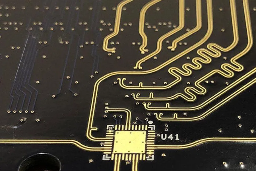
A core requirement of RF PCB design software is the ability to create layouts optimized for high-frequency signals. This includes tools for precise trace routing, controlled impedance traces, and proper spacing to minimize interference. High-frequency PCB layout tools allow you to define specific trace widths and lengths to maintain consistent signal paths, often down to tolerances of 0.1 mm or less.
For instance, at frequencies above 1 GHz, even a small deviation in trace length can cause phase shifts, disrupting signal timing. Good software will let you simulate and adjust these layouts in real-time, ensuring your design meets performance goals before manufacturing.
Additionally, look for features that support multi-layer designs, as RF PCBs often use multiple ground planes to reduce noise. The software should allow you to visualize and manage these layers easily, ensuring proper alignment and connection through vias.
2. Impedance Matching Tools for RF Design
Impedance matching is critical in RF applications to prevent signal reflections and maximize power transfer. Without proper matching, a system operating at 2.4 GHz (a common frequency for wireless communication) could lose up to 50% of its signal power due to reflections. RF PCB design software must include impedance matching tools to calculate and adjust trace impedance accurately.
These tools often integrate calculators for determining the characteristic impedance of traces based on factors like trace width, thickness, and the dielectric constant of the substrate material. For example, a typical 50-ohm impedance line on a standard FR-4 substrate might require a trace width of approximately 1.8 mm at a specific board thickness. The software should allow you to input these parameters and visualize the results instantly.
Advanced software may also offer simulation features to test impedance matching under different conditions, helping you fine-tune your design before production. This capability is invaluable for PCB design for wireless communication, where signal integrity is non-negotiable.
3. Signal Integrity Analysis for RF
Signal integrity for RF is another cornerstone of effective PCB design. High-frequency signals are prone to issues like crosstalk, noise, and signal degradation, especially in compact designs with closely spaced traces. RF PCB design software should include robust signal integrity analysis tools to identify and mitigate these problems early in the design process.
Look for features that simulate signal behavior at high frequencies, such as eye diagrams and time-domain reflectometry (TDR) analysis. These tools can predict how a signal will perform at speeds of 10 Gbps or higher, helping you spot potential issues like overshoot or ringing. Some software even provides 3D electromagnetic (EM) simulation to model how signals interact with the board's physical structure, offering a deeper level of insight.
For wireless communication projects, signal integrity analysis ensures that data transmission remains reliable, even in noisy environments. This is especially important for applications like 5G, where signal quality directly impacts performance.
4. Support for High-Frequency Materials
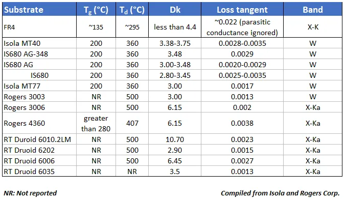
RF PCBs often require specialized materials with low dielectric constants (Dk) and low loss tangents to maintain signal quality. Common materials like FR-4 may not suffice for frequencies above 1 GHz due to their higher loss characteristics. Instead, materials with Dk values between 2.2 and 3.5 and loss tangents below 0.005 are often used to ensure signal velocity and impedance consistency.
Your RF PCB design software should support libraries or databases of high-frequency materials, allowing you to select the right substrate for your project. It should also account for material properties during simulations, ensuring that your design performs as expected in real-world conditions. For example, the software might help you calculate how a material with a Dk of 3.0 affects trace impedance compared to one with a Dk of 4.5.
This feature is crucial for engineers working on PCB design for wireless communication, where material selection can make or break a project's success.
5. Electromagnetic Compatibility (EMC) and EMI Mitigation Tools
High-frequency designs are highly susceptible to electromagnetic interference (EMI), which can disrupt signal performance and cause compliance issues. RF PCB design software should offer tools to analyze and mitigate EMI, ensuring electromagnetic compatibility (EMC) with regulatory standards.
These tools might include features for simulating near-field and far-field radiation patterns, helping you identify potential interference sources. Some software also suggests layout adjustments, like adding shielding or optimizing ground plane placement, to reduce EMI. For instance, ensuring a continuous ground plane under RF traces can reduce noise by up to 30% in some designs.
EMC tools are especially important for wireless communication devices, which must operate without interfering with other nearby electronics. Software with built-in compliance checks can save time and prevent costly redesigns.
6. Integration with Simulation and Testing Tools
Simulation is a vital part of RF design, allowing engineers to test their layouts virtually before manufacturing. The best RF PCB design software integrates seamlessly with simulation tools for circuit analysis, thermal management, and RF performance. This integration lets you validate your design under realistic conditions, reducing the risk of errors.
For example, thermal simulations can predict how heat dissipation affects high-frequency components, while RF simulations can model signal behavior at frequencies up to 10 GHz or beyond. Some software even supports co-simulation, combining electrical and mechanical analysis for a holistic view of your design.
This feature is a game-changer for high-frequency PCB layout, as it helps you catch issues early and iterate quickly, saving time and resources.
Additional Considerations for Choosing RF PCB Design Software
Beyond the core features, there are a few additional factors to keep in mind when selecting software for RF applications. These can enhance your workflow and ensure long-term success.
User-Friendly Interface and Learning Curve
RF design is complex enough without struggling with clunky software. Look for a platform with an intuitive interface and comprehensive documentation or tutorials. A shorter learning curve means you can start designing sooner and focus on solving technical challenges rather than navigating the tool.
Scalability for Future Projects
As your projects grow in complexity, your software should keep up. Choose a tool that supports larger, more intricate designs and offers regular updates to stay compatible with emerging technologies like 5G or IoT.
Community and Support Resources
Access to a strong user community or technical support can be a lifesaver when you're stuck on a tricky design problem. Software with active forums, webinars, or direct support channels ensures you’re never left without help.
How These Features Benefit RF PCB Design for Wireless Communication
Wireless communication systems, such as Wi-Fi, Bluetooth, and 5G devices, rely heavily on RF PCBs for reliable performance. The features discussed above directly impact the success of these applications. For instance, impedance matching tools ensure efficient power transfer in antennas, while signal integrity analysis prevents data loss during high-speed transmission. High-frequency PCB layout tools help create compact, efficient designs that fit into small devices without sacrificing performance.
By using software with these capabilities, engineers can design PCBs that meet the stringent demands of modern wireless communication, delivering faster, more reliable connections in an increasingly connected world.
Conclusion: Building Better RF PCBs with the Right Software
Designing PCBs for RF applications is a specialized field that requires the right tools to succeed. RF PCB design software with features like high-frequency PCB layout tools, impedance matching capabilities, signal integrity analysis, and support for high-frequency materials is essential for creating reliable, high-performance circuits. These tools not only address the unique challenges of RF design but also streamline the process, saving time and reducing errors.
Whether you're working on PCB design for wireless communication or other high-frequency projects, choosing software with these essential features ensures your designs meet performance and compliance standards. By focusing on precision, simulation, and material compatibility, you can tackle even the most complex RF challenges with confidence.
At ALLPCB, we understand the importance of precision in RF PCB design. Our services are tailored to support engineers in bringing their high-frequency projects to life with quality and efficiency. Explore the right tools and resources to elevate your next RF design, and let us help you achieve outstanding results.