 ALLPCB


Designing a printed circuit board (PCB) for USB interfaces can be challenging, especially when it comes to managing constraints to ensure signal integrity and compliance with standards. Whether you're working on USB 2.0, USB 3.0, or even the latest USB-C designs, understanding USB PCB design constraints, USB routing rules, impedance control for USB, differential pairs in USB, and signal integrity for USB is critical to creating a reliable and high-performing product. In this comprehensive guide, we’ll dive deep into the essential aspects of PCB constraint management for USB designs, providing practical tips and actionable insights to help engineers achieve optimal results.
Why PCB Constraint Management Matters for USB Designs
USB technology is widely used in countless devices, from smartphones to industrial equipment, thanks to its versatility and speed. However, as data rates increase—USB 2.0 operates at 480 Mbps, USB 3.0 at 5 Gbps, and USB 3.2 at up to 20 Gbps—maintaining signal integrity becomes more complex. Poorly managed PCB constraints can lead to issues like signal distortion, crosstalk, and electromagnetic interference (EMI), resulting in data errors or device failures. Proper constraint management ensures that your USB design meets performance standards and complies with industry specifications.
In this blog, we’ll break down the key constraints for USB PCB designs and provide clear guidelines to help you avoid common pitfalls. Let’s start by exploring the fundamental elements of USB design constraints.
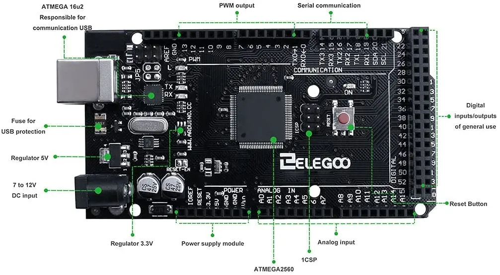
Suggested Image Placement: Place an image here showing a USB PCB layout with labeled differential pairs and connectors.
Understanding USB PCB Design Constraints
USB PCB design constraints refer to the rules and limitations that govern how traces, components, and layers are arranged on a board to ensure proper functionality. These constraints are driven by the need to maintain signal integrity, minimize noise, and adhere to USB standards. Here are the primary constraints to consider:
- Trace Length and Matching: USB signals, especially high-speed ones, require precise trace length matching to prevent timing errors. For USB 2.0, the differential pair traces (D+ and D-) should be matched within 150 mils (3.81 mm) of each other. For USB 3.0 and above, this tolerance tightens to around 10-15 mils (0.25-0.38 mm) due to higher data rates.
- Impedance Control: USB designs rely on controlled impedance to ensure signal quality. USB 2.0 differential pairs typically require a differential impedance of 90 ohms (±15%), while USB 3.0 and higher standards often specify 85 ohms (±10%).
- Layer Stackup: The PCB layer stackup affects signal integrity. High-speed USB signals often require a 4-layer or higher PCB with dedicated ground and power planes to reduce noise and provide a stable return path.
- Connector Placement: USB connectors must be placed to minimize signal path length and avoid interference from other components. Keep high-speed traces as short and direct as possible.
By adhering to these USB PCB design constraints, you can reduce the risk of signal degradation and ensure compliance with USB specifications.
Key USB Routing Rules for Optimal Performance
Routing is one of the most critical aspects of USB PCB design. Improper routing can lead to signal reflections, crosstalk, and EMI issues. Below are some essential USB routing rules to follow:
- Route Differential Pairs Together: USB signals are transmitted over differential pairs (D+ and D- for USB 2.0, and additional pairs for USB 3.0). These traces must be routed side by side with consistent spacing to maintain signal integrity. A typical spacing for USB 2.0 differential pairs is 5-8 mils (0.127-0.203 mm) between the traces, depending on the PCB material and stackup.
- Avoid Sharp Corners: Use 45-degree angles or smooth curves instead of 90-degree bends when routing USB traces. Sharp corners can cause signal reflections and degrade performance.
- Minimize Via Usage: Vias introduce impedance discontinuities and can affect signal quality. If vias are necessary, keep them to a minimum and ensure they are placed symmetrically for differential pairs.
- Keep Traces Away from Noise Sources: Route USB traces away from high-frequency components, power lines, and other potential sources of interference. Maintain a clearance of at least 20 mils (0.508 mm) from other signals.
- Ground Plane Continuity: Ensure a continuous ground plane beneath USB traces to provide a low-impedance return path. Avoid splitting ground planes under differential pairs, as this can lead to noise coupling.
Following these USB routing rules helps maintain signal integrity and reduces the likelihood of data errors in your USB design.
Related Reading: Differential Pair Routing: Techniques for High-Speed PCB Layouts
Impedance Control for USB: Why It’s Critical
Impedance control for USB is a cornerstone of high-speed PCB design. Impedance mismatches can cause signal reflections, leading to data loss and reduced performance. For USB designs, differential impedance is the key parameter to manage. Here’s how to achieve proper impedance control:
- Calculate Trace Width and Spacing: Use an impedance calculator or simulation tool to determine the correct trace width and spacing for your PCB stackup. For a standard FR-4 material with a dielectric constant of 4.2-4.5, a USB 2.0 differential pair might require a trace width of 6 mils (0.152 mm) and spacing of 8 mils (0.203 mm) on a 4-layer board to achieve 90 ohms differential impedance.
- Choose the Right PCB Material: The dielectric constant of the PCB material affects impedance. FR-4 is commonly used for USB 2.0, but for USB 3.0 and higher, consider low-loss materials like Rogers or Isola to maintain signal quality at higher frequencies.
- Work with Your Manufacturer: Collaborate with your PCB fabrication team to ensure they can meet the required impedance tolerances. Many manufacturers offer controlled impedance testing to verify the final product.
Proper impedance control for USB ensures that signals travel without distortion, maintaining the high-speed performance expected from USB interfaces.
Related Reading: PCB Design for USB Interfaces: Ensuring Reliable Data Transfer
Differential Pairs in USB: Best Practices for Routing
Differential pairs in USB are critical for high-speed data transmission. These pairs carry complementary signals that cancel out noise when routed correctly. Here are some best practices for managing differential pairs in USB designs:
- Length Matching: As mentioned earlier, the traces in a differential pair must be of equal length to prevent skew. For USB 3.0, aim for length matching within 10 mils (0.254 mm) to avoid timing issues at 5 Gbps or higher.
- Symmetrical Routing: Route both traces of a differential pair symmetrically, maintaining equal spacing and avoiding obstacles that could disrupt one trace more than the other.
- Reference Planes: Ensure that differential pairs are routed over a continuous ground or power plane. This provides a stable reference and reduces EMI.
- Coupling: Keep the traces tightly coupled (close together) to minimize external noise pickup. Loose coupling can increase susceptibility to interference.
By following these guidelines for differential pairs in USB, you can significantly improve the reliability of your USB data transmission.
Ensuring Signal Integrity for USB Designs
Signal integrity for USB is the ultimate goal of constraint management. Signal integrity refers to the ability of a signal to maintain its quality as it travels through the PCB, without distortion or interference. Here are key strategies to ensure signal integrity for USB:
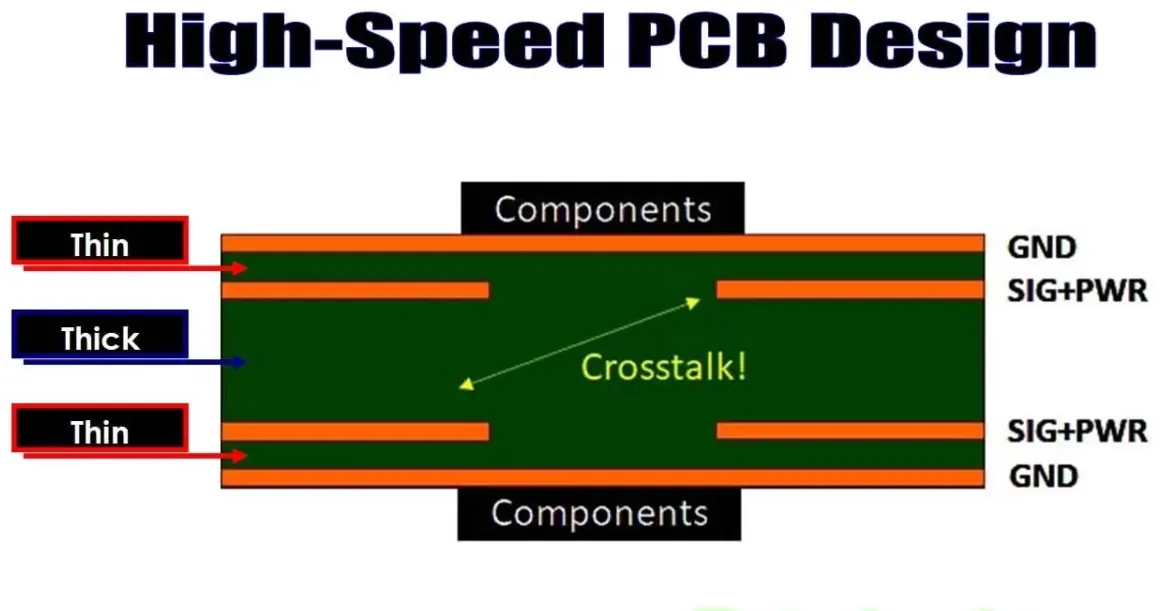
- Minimize Crosstalk: Crosstalk occurs when signals from adjacent traces interfere with each other. Maintain sufficient spacing between USB traces and other high-speed signals—typically at least 3 times the trace width (e.g., 18 mils or 0.457 mm for a 6-mil trace).
- Control Reflections: Reflections are caused by impedance mismatches. Use termination resistors if necessary, especially for longer USB traces, to match the impedance at the end of the line.
- Reduce EMI: Electromagnetic interference can disrupt USB signals. Use shielding techniques, such as adding ground vias around USB traces, to contain EMI. Also, ensure proper grounding of the USB connector shell.
- Simulation and Testing: Use signal integrity simulation tools to model your USB design before fabrication. After manufacturing, perform tests like eye diagram analysis to verify signal quality. For USB 2.0, the eye diagram should show a clear opening with minimal jitter (typically less than 100 ps).
By prioritizing signal integrity for USB, you can ensure that your design performs reliably even under demanding conditions.
Compliance with USB Standards
Beyond signal integrity, your USB PCB design must comply with industry standards set by the USB Implementers Forum (USB-IF). Compliance ensures interoperability and reliability across devices. Key compliance considerations include:
- Electrical Specifications: Meet the voltage and current requirements for USB power delivery. For example, USB 2.0 supports up to 5V at 500 mA, while USB-C with Power Delivery can handle up to 20V at 5A.
- Connector and Cable Testing: Ensure that your design passes USB-IF certification tests for connectors and cables, which include signal integrity and mechanical durability checks.
- Protocol Compliance: Verify that your design adheres to the USB protocol for data transfer, including proper enumeration and error handling.
Compliance testing can be complex, so consider working with a certified lab or using pre-certified components to streamline the process.
Common Challenges and Solutions in USB PCB Design
Even with careful planning, USB PCB designs can face challenges. Here are some common issues and how to address them:
- Signal Skew: Caused by unequal trace lengths in differential pairs. Solution: Use length-matching techniques and design software with automated length-tuning features.
- High EMI: Often due to poor grounding or trace routing near noise sources. Solution: Add ground shielding and route traces away from noisy components.
- Impedance Mismatch: Results from incorrect trace dimensions or PCB material variations. Solution: Use impedance calculators and work with your manufacturer to ensure consistency.
By anticipating these challenges and applying the right solutions, you can avoid costly redesigns and delays.
Conclusion: Mastering USB PCB Constraint Management
Effective PCB constraint management is the foundation of successful USB designs. By understanding and applying USB PCB design constraints, following USB routing rules, ensuring impedance control for USB, managing differential pairs in USB, and prioritizing signal integrity for USB, you can create reliable, high-performance USB interfaces that meet industry standards. Whether you're designing for USB 2.0 or the latest USB-C, these principles will guide you toward a successful outcome.
At ALLPCB, we’re committed to supporting engineers with the tools and resources needed for cutting-edge PCB designs. With careful planning, precise execution, and a focus on compliance, your USB designs can achieve optimal performance and reliability. Start applying these guidelines today to elevate your next project!


