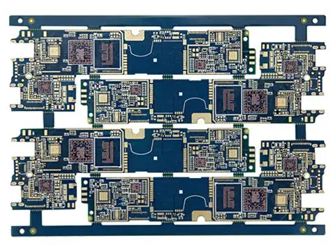
Designing a printed circuit board (PCB) can be a complex task, but using established PCB design standards is a proven way to avoid costly manufacturing errors. By following guidelines like a PCB DFM checklist (Design for Manufacturability), you can prevent manufacturing errors, reduce PCB rework, optimize PCB yield, and minimize PCB scrap. In this comprehensive guide, we’ll walk you through the importance of design standards and provide actionable steps to ensure your PCB projects are successful and cost-effective.
Why PCB Design Standards Matter for Manufacturing Success
PCB design standards act as a roadmap for engineers to create boards that are not only functional but also easy to manufacture. Without these guidelines, small oversights in the design phase can lead to big problems during production, such as misaligned components, insufficient clearances, or even complete board failures. These errors often result in costly rework, delays, or scrapped materials.
By adhering to industry standards, such as those set by the Institute of Printed Circuits (IPC), you can catch potential issues early. For instance, ensuring proper trace widths (e.g., a minimum of 6 mils for standard designs) and spacing (e.g., at least 8 mils between traces for 1 oz copper) can prevent short circuits during manufacturing. This proactive approach directly impacts your bottom line by optimizing PCB yield and minimizing PCB scrap.

What Are PCB Design Standards and DFM Guidelines?
PCB design standards are a set of rules and best practices that guide the layout and production of circuit boards. These standards, often developed by organizations like IPC, cover everything from material selection to component placement and electrical performance. Design for Manufacturability (DFM) guidelines are a subset of these standards, focusing specifically on making sure the design can be produced efficiently and without errors.
A PCB DFM checklist is a critical tool in this process. It includes checks for minimum trace widths, drill hole sizes, and pad-to-pad clearances to ensure the design aligns with manufacturing capabilities. For example, a common DFM rule is to maintain a minimum annular ring of 5 mils around vias to avoid drilling issues. Following such a checklist helps in preventing manufacturing errors before they occur.
Key Benefits of Using PCB Design Standards
Implementing PCB design standards offers several advantages that directly contribute to reducing PCB rework and improving overall project outcomes. Here are some key benefits:
- Error Prevention: Standards help identify potential issues, like insufficient solder mask clearance (e.g., less than 4 mils), during the design phase rather than after production.
- Cost Reduction: By catching errors early, you avoid expensive rework or scrap, which can cost thousands of dollars for high-volume runs.
- Improved Yield: Optimizing PCB yield means more usable boards per production batch, achieved by adhering to DFM rules like proper panelization.
- Faster Turnaround: A design that meets manufacturing standards reduces back-and-forth communication with fabricators, speeding up the process.
Common Manufacturing Errors and How Standards Prevent Them
Manufacturing errors can stem from various design oversights. Let’s explore some common issues and how PCB design standards help avoid them:
1. Incorrect Component Placement
Placing components too close together can lead to soldering issues or thermal problems. For instance, if two high-power components are placed without at least 50 mils of spacing, heat dissipation becomes a challenge, potentially causing failures. DFM guidelines recommend specific clearances based on component types and board density to prevent such issues.
2. Insufficient Trace Widths and Spacing
Traces that are too narrow or spaced too closely can result in short circuits or signal interference. A standard rule for 1 oz copper is a minimum trace width of 6 mils and spacing of 8 mils. Adhering to these limits ensures the board can handle the required current without risk during fabrication.
3. Misaligned Vias and Drill Holes
Vias or drill holes that are not properly aligned with pads can cause connectivity issues. A DFM checklist often specifies a minimum annular ring of 5 mils around vias to ensure accurate drilling. This small detail can save entire batches from becoming scrap.
4. Poor Solder Mask Application
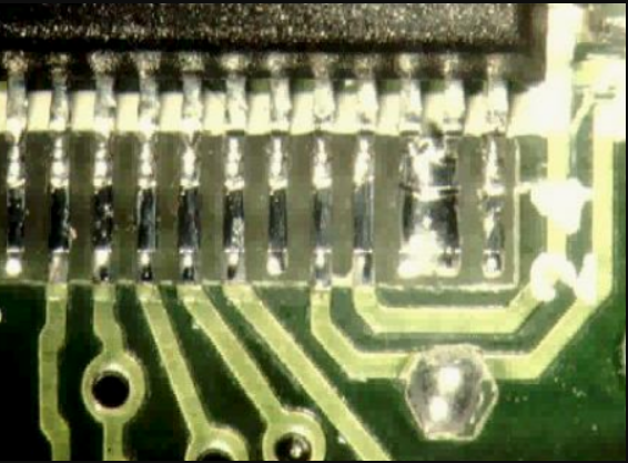
Inadequate solder mask clearance around pads can lead to solder bridging during assembly. Standards suggest a clearance of at least 4 mils to avoid this, ensuring clean and reliable soldering.
A Comprehensive PCB DFM Checklist for Preventing Manufacturing Errors
To help you get started, here’s a practical PCB DFM checklist that focuses on preventing manufacturing errors and optimizing PCB yield. Use this as a guide during your design process:
- Trace and Spacing: Ensure minimum trace width (e.g., 6 mils for 1 oz copper) and spacing (e.g., 8 mils) to avoid shorts and signal issues.
- Via Design: Maintain a minimum annular ring of 5 mils and avoid placing vias under components unless necessary.
- Component Clearance: Keep at least 50 mils between high-power components for heat dissipation and 20 mils for standard components to ease assembly.
- Solder Mask: Apply a clearance of at least 4 mils around pads to prevent solder bridging.
- Drill Holes: Use standard drill sizes (e.g., 10 mils or larger) to match manufacturing capabilities and avoid custom tooling costs.
- Board Edge Clearance: Keep components and traces at least 10 mils away from board edges to prevent damage during depanelization.
- Panelization: Optimize board layout on the panel to maximize yield and reduce material waste.
- Documentation: Provide clear layer stackup details and fabrication notes to avoid miscommunication with manufacturers.
By following this checklist, you can significantly reduce the chances of errors and minimize PCB scrap during production.
Steps to Implement PCB Design Standards in Your Workflow
Integrating design standards into your process doesn’t have to be complicated. Here are actionable steps to ensure your designs are ready for manufacturing:
1. Use Design Rule Checking (DRC) Tools
Most PCB design software includes automated Design Rule Checking (DRC) tools. These tools scan your layout for violations like insufficient spacing or incorrect via sizes based on predefined standards. Set up rules with specific values, such as a minimum trace width of 6 mils, to catch errors early.
2. Collaborate with Manufacturers Early
Reach out to your manufacturing partner during the design phase to understand their specific capabilities and constraints. For example, if their minimum drill size is 10 mils, adjust your design accordingly to avoid production delays.
3. Test with Prototypes
Before full-scale production, create a prototype to test your design under real-world conditions. This step helps identify issues like signal integrity problems (e.g., impedance mismatches at 50 ohms for high-speed signals) that might not be apparent in simulations.
4. Document Everything Clearly
Provide detailed fabrication and assembly notes, including layer stackup information and material specifications. Clear documentation prevents misinterpretation, reducing PCB rework.
How Standards Optimize PCB Yield and Minimize Scrap
Optimizing PCB yield is all about getting the maximum number of usable boards from each production run. Design standards play a huge role in this by ensuring consistency and manufacturability. For instance, proper panelization—arranging multiple boards on a single panel—can increase yield by up to 20% by reducing material waste. Standards also guide the use of standard via sizes (e.g., 10 mils) to avoid custom tooling, which can introduce errors and increase scrap rates.
Minimizing PCB scrap also ties directly to cost savings. If a batch of 1,000 boards has a 5% scrap rate due to design errors, that’s 50 unusable boards. At $10 per board, that’s $500 lost. Following a PCB DFM checklist can bring that scrap rate down to 1% or less, saving significant resources.
Real-World Example: Reducing Rework with Standards
Consider a scenario where a company designs a multilayer PCB for a consumer device. Initially, they ignored DFM guidelines, resulting in a 10% rework rate due to issues like insufficient solder mask clearance and misaligned vias. After implementing a strict PCB DFM checklist and using DRC tools, they reduced rework to under 2%. This not only saved them thousands in production costs but also sped up their time-to-market by two weeks.
This example shows how small changes, guided by design standards, can have a big impact on preventing manufacturing errors and reducing PCB rework.
Final Thoughts on Using PCB Design Standards
Using PCB design standards is a smart strategy for any engineer looking to avoid costly manufacturing errors. By following a PCB DFM checklist, you can prevent issues before they arise, optimize PCB yield, and minimize PCB scrap. These standards provide a clear framework for creating designs that are both functional and manufacturable, saving time and money in the long run.
Start by integrating tools like DRC into your workflow, collaborating with manufacturers, and sticking to industry guidelines. With these steps, you’ll be well on your way to producing high-quality PCBs with fewer headaches and better results. Whether you’re working on a small prototype or a large production run, the principles of preventing manufacturing errors and reducing rework remain the same—design with standards in mind
 ALLPCB


