ALLPCB


The rapid evolution of technology has thrust high-speed PCB (Printed Circuit Board) design into the spotlight, especially with the rise of IoT (Internet of Things) and 5G applications. These cutting-edge fields demand faster data rates, higher frequencies, and compact designs—pushing engineers to navigate a maze of challenges like signal integrity, thermal management, and electromagnetic interference (EMI). For engineers working on next-generation devices, mastering high-speed PCB design is no longer optional; it's a necessity to keep pace with innovation.
At its core, high-speed PCB design is about ensuring reliable performance when signals travel at lightning speeds—think edge rates below 1 nanosecond or frequencies exceeding 50 MHz. Whether it's a smart sensor in an IoT network or a 5G base station handling millimeter-wave signals, the stakes are high. In this blog, we'll dive into the key challenges engineers face in these applications and share practical solutions to overcome them. Let's explore how to turn complexity into opportunity.
Understanding High-Speed PCB Design in IoT and 5G
High-speed PCB design refers to layouts optimized for fast signal transitions and high-frequency operations. Unlike traditional PCBs, where signal speeds were slower and tolerances looser, high-speed designs must account for effects like signal reflection, crosstalk, and impedance mismatches. In IoT, devices often juggle multiple wireless protocols (e.g., Wi-Fi, Bluetooth, NB-IoT) in tiny form factors. Meanwhile, 5G pushes the envelope with frequencies up to 77 GHz and data rates reaching 20 Gbps—demanding precision at every layer of the board.
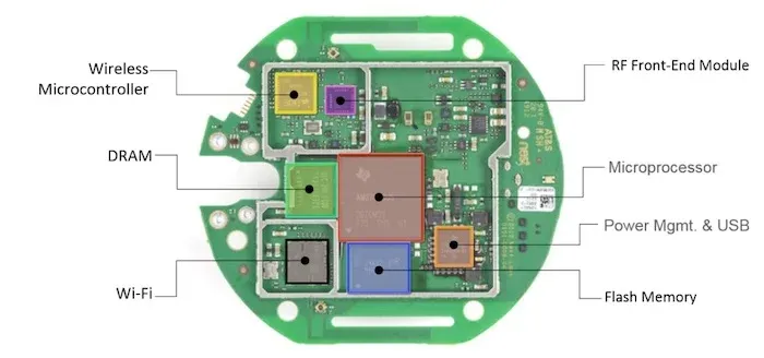
For IoT, the challenge is packing power-efficient, mixed-signal circuits into small spaces. A smart thermostat, for instance, might integrate a 2.4 GHz Wi-Fi module, a low-power microcontroller, and sensors—all on a board smaller than a credit card. In 5G, the focus shifts to handling millimeter-wave signals (above 24 GHz), which are sensitive to even minor design flaws. Both applications share a need for speed, but their unique requirements—miniaturization for IoT, high bandwidth for 5G—shape the obstacles engineers must tackle.
Key Challenges in High-Speed PCB Design
Signal Integrity: Keeping Data Intact
Signal integrity (SI) is the cornerstone of high-speed design. At high frequencies, signals can degrade due to reflections, crosstalk, or attenuation. For example, a 5G PCB operating at 28 GHz might see a signal weaken by 0.5 dB per inch of trace length if not properly managed. In IoT, a poorly routed trace between a sensor and processor could introduce noise, corrupting data.
The root causes? Impedance mismatches and long trace lengths. A typical high-speed signal requires a controlled impedance of 50 ohms (single-ended) or 100 ohms (differential). Deviations as small as 10% can cause reflections, reducing signal quality. In 5G, millimeter waves amplify this issue due to their short wavelengths—about 1 mm at 30 GHz—making even tiny layout errors significant.
Thermal Management: Handling the Heat
High-speed components like 5G power amplifiers or IoT microprocessors generate heat—lots of it. A 5G base station's RF front-end might dissipate 10-20 watts, while an IoT device's compact design leaves little room for airflow. Without proper PCB thermal management, temperatures can soar past 85°C, degrading performance or causing failure.
Materials play a big role here. Standard FR-4 substrates, with a thermal conductivity of 0.3 W/m·K, struggle to dissipate heat in high-speed designs. Compare that to advanced laminates like Rogers RO4350B, offering 0.6 W/m·K, and the difference is clear. Engineers must balance cost and performance when choosing materials, especially in cost-sensitive IoT applications.
Electromagnetic Interference (EMI): Taming the Noise
EMI is a silent killer in high-speed PCBs. In 5G, frequencies above 6 GHz can radiate energy, interfering with nearby circuits. In IoT, mixed-signal designs—combining analog sensors and digital processors—heighten the risk of crosstalk. For instance, a 2.4 GHz Wi-Fi signal could couple with a nearby power line, introducing noise that disrupts data transmission.
The stakes are high: EMI violations can fail FCC compliance tests, delaying product launches. At 28 GHz, a 5G signal's skin depth drops to 0.4 micrometers, meaning current hugs the surface of copper traces. Rough traces amplify losses and EMI, making manufacturing precision critical.
Miniaturization: Fitting More in Less Space
IoT devices thrive on small footprints. A wearable fitness tracker, for example, might cram a 5 mm x 5 mm microcontroller, a 3 mm x 3 mm antenna, and a battery onto a 20 mm x 30 mm board. High-speed signals complicate this, as shorter traces (to reduce losses) clash with the need for component spacing. In 5G, phased array antennas—essential for beamforming—demand tight layouts, often requiring high-density interconnect (HDI) techniques with vias as small as 0.1 mm.
Overcoming High-Speed PCB Design Challenges
Mastering Signal Integrity
To maintain signal integrity, controlled impedance is non-negotiable. Use a stackup with consistent dielectric thickness—say, 0.1 mm between layers—and calculate trace widths accurately. For a 50-ohm impedance on FR-4 (dielectric constant ~4.5), a 0.15 mm trace width might suffice, but tools like a field solver can refine this based on your stackup.
Shorten trace lengths where possible. In 5G, keep traces under 10 mm for 28 GHz signals to minimize attenuation. Differential pairs, common in high-speed designs, should be routed with equal lengths (within 0.1 mm) to avoid skew. Ground planes beneath traces shield against crosstalk, while vias should be minimized—each one adds 0.5-1 nH of inductance, disrupting signals.
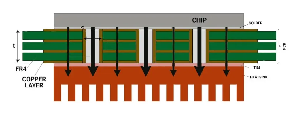
Cooling the Heat
Thermal vias are a go-to solution. A grid of 0.3 mm vias under a hot component can cut temperatures by 10-15°C by conducting heat to a copper plane. For 5G, consider metal-core PCBs or heat sinks if power exceeds 5 watts. In IoT, low-power modes—like shutting off a Wi-Fi module when idle—reduce heat while preserving battery life. Materials like Isola IS680 (thermal conductivity ~0.5 W/m·K) strike a balance between cost and performance.
Reducing EMI
Start with a solid ground plane—split planes invite noise. For 5G, use smooth copper (e.g., rolled annealed copper) with a roughness below 0.5 micrometers to limit skin effect losses. In IoT, separate analog and digital sections with a 1 mm gap, and route high-speed traces away from edges to curb radiation. Shielding cans or conductive gaskets can tame stubborn EMI, though they add cost and complexity.
Tackling Miniaturization
HDI technology is a game-changer. Microvias (0.1 mm diameter) and buried vias shrink layer counts, freeing space. In IoT, flexible PCBs adapt to odd shapes—like a curved wearable—while maintaining signal integrity. For 5G, integrate antennas directly onto the PCB, reducing external components. A 4x4 MIMO array, for instance, can fit on a 20 mm x 20 mm board with careful planning.
Material Selection: The Foundation of Success
Choosing the right substrate is critical. FR-4 works for IoT at 2.4 GHz, but its dielectric constant (Dk) of 4.5 and loss tangent of 0.02 cause signal loss above 6 GHz. For 5G, low-Dk materials like Rogers RT/duroid 5880 (Dk ~2.2, loss tangent ~0.0009) excel at 28 GHz and beyond. These materials cost more—up to 10x FR-4—but deliver unmatched performance.
Hybrid stackups blend cost and capability. Pair FR-4 with a high-frequency laminate for RF layers, keeping digital sections affordable. In IoT, thin substrates (0.2 mm) save space, but ensure they handle thermal stress—delamination at 120°C is a risk with cheap materials.
Design Tools and Best Practices
Simulation tools like Cadence or Altium's signal integrity analyzers catch issues early. Model a 5G trace at 28 GHz to spot reflections, or simulate an IoT board's power distribution to avoid voltage drops. Follow these best practices:
- Layer Planning: Dedicate layers to ground and power for stability.
- Trace Routing: Use 45-degree angles, not 90-degree bends, to reduce reflections.
- Component Placement: Group high-speed parts near connectors to shorten paths.
Testing is key. A network analyzer can verify impedance (target: ±10% of 50 ohms), while thermal cameras pinpoint hot spots. Iterate designs based on real-world data—simulations aren't foolproof.
How ALLPCB Supports High-Speed Design
For engineers tackling these challenges, partnering with a reliable manufacturer can make all the difference. ALLPCB offers quick-turn prototyping—think 24-hour turnarounds—letting you test and refine high-speed designs fast. Our advanced manufacturing handles HDI, flexible PCBs, and tight tolerances (down to 0.1 mm vias), perfect for IoT and 5G. Plus, with global logistics, your boards arrive on time, anywhere. Whether you're perfecting a 5G antenna or shrinking an IoT sensor, we've got the tools and expertise to bring your vision to life.
Conclusion: Turning Challenges into Innovation
High-speed PCB design for IoT and 5G is a balancing act—signal integrity, heat, EMI, and size all demand attention. By mastering impedance control, leveraging advanced materials, and embracing HDI, engineers can conquer these hurdles. The reward? Devices that push boundaries, from smart cities powered by IoT to lightning-fast 5G networks.
The future is fast, and we're here to help you keep up. What's your next high-speed project? Dive in, experiment, and let precision drive your success.