 ALLPCB


In the rapidly evolving world of electronics, flexible PCBs (Printed Circuit Boards) are becoming a game-changer for creating bendable and lightweight devices. Whether you're an engineer working on wearables, medical devices, or automotive systems, understanding the tools and techniques for designing flexible PCBs is essential. This comprehensive guide dives into flexible PCB design software, flex PCB materials, flex PCB bending techniques, flex PCB adhesive selection, flex PCB connector types, flex PCB manufacturing process, designing for dynamic bending, and rigid-flex PCB design tools. Let’s explore how to bring your innovative ideas to life with the right tools and strategies.
What Are Flexible PCBs and Why Do They Matter?
Flexible PCBs, often called flex circuits, are thin, lightweight circuit boards that can bend and conform to unique shapes. Unlike rigid PCBs, they use flexible substrates like polyimide, allowing them to fit into tight spaces or endure repeated bending in dynamic applications. Their importance lies in enabling compact designs for modern electronics, from smartwatches to aerospace components.
Designing for bendable electronics requires specialized tools and knowledge. In this blog, we’ll break down the essentials to help you navigate the process, ensuring your designs are both functional and reliable.
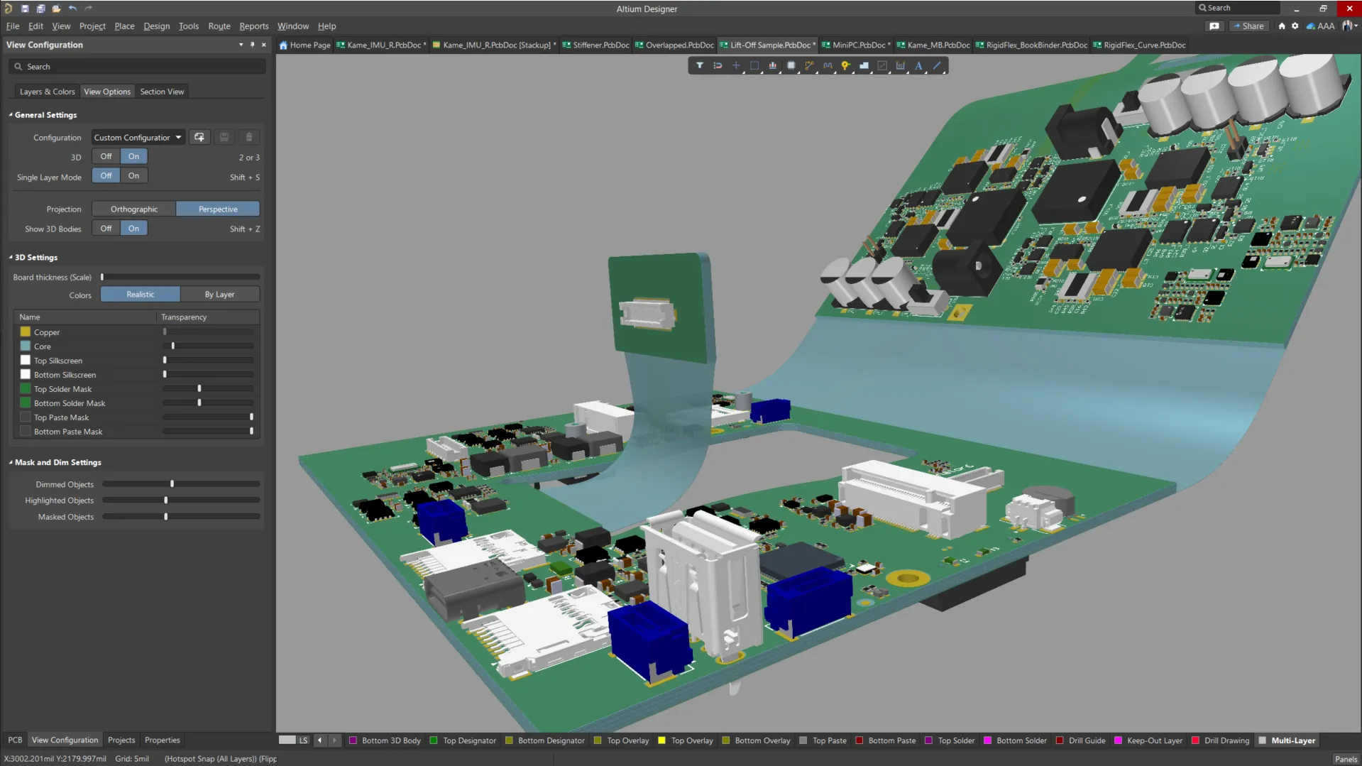
Flexible PCB Design Software: Tools to Get Started
Choosing the right flexible PCB design software is the foundation of a successful project. These tools help you create layouts that account for bending, material properties, and electrical performance. Here are some key features to look for in design software tailored for flex circuits:
- 3D Modeling Capabilities: Since flex PCBs often need to fit into irregular shapes, software with 3D visualization helps simulate how the board will bend and fit in the final product.
- Material Libraries: Access to databases with flexible substrate properties ensures accurate simulations of stress and strain.
- Dynamic Bending Analysis: Tools that predict how traces and components behave under bending stress are critical for durability.
Popular software categories include those with advanced simulation features for signal integrity (important for high-speed signals often exceeding 1 GHz) and thermal management. For instance, ensuring impedance control—typically targeting values like 50 ohms for RF applications—is easier with software that supports detailed stack-up configurations.
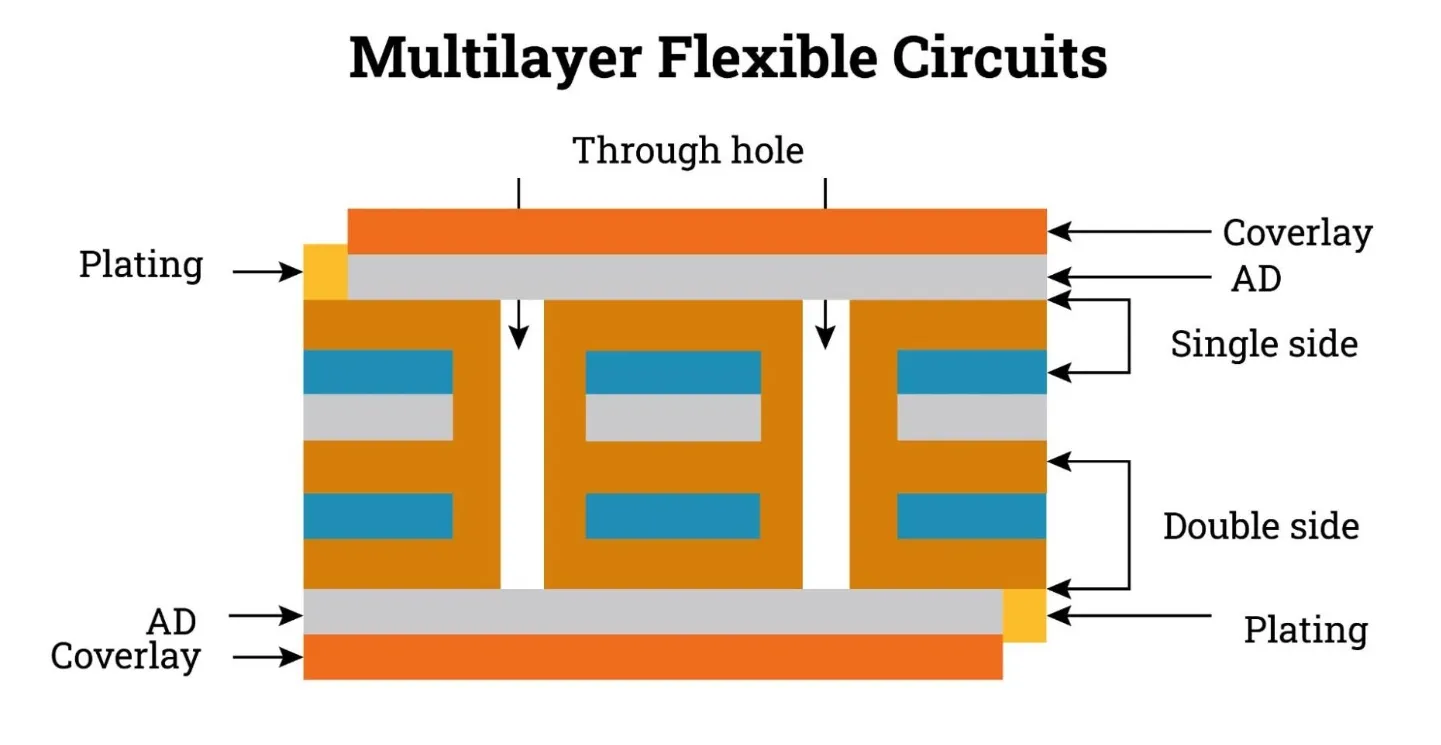
Flex PCB Materials: Building Blocks of Bendable Designs
The choice of flex PCB materials directly impacts performance, durability, and cost. The most common substrate for flexible circuits is polyimide, known for its high thermal stability (up to 260°C) and flexibility. Here’s a breakdown of key materials:
- Substrates: Polyimide films, typically 12.5 to 50 micrometers thick, provide the base layer. They resist cracking even after thousands of bending cycles.
- Conductors: Rolled annealed copper foil, often 18 to 35 micrometers thick, is preferred over electrodeposited copper due to its better flexibility and fatigue resistance.
- Coverlays: These protective layers, also made of polyimide, shield traces from environmental damage while maintaining flexibility.
Selecting materials involves balancing flexibility with electrical needs. For example, thinner copper reduces weight but may increase resistance, affecting signal integrity at high frequencies.
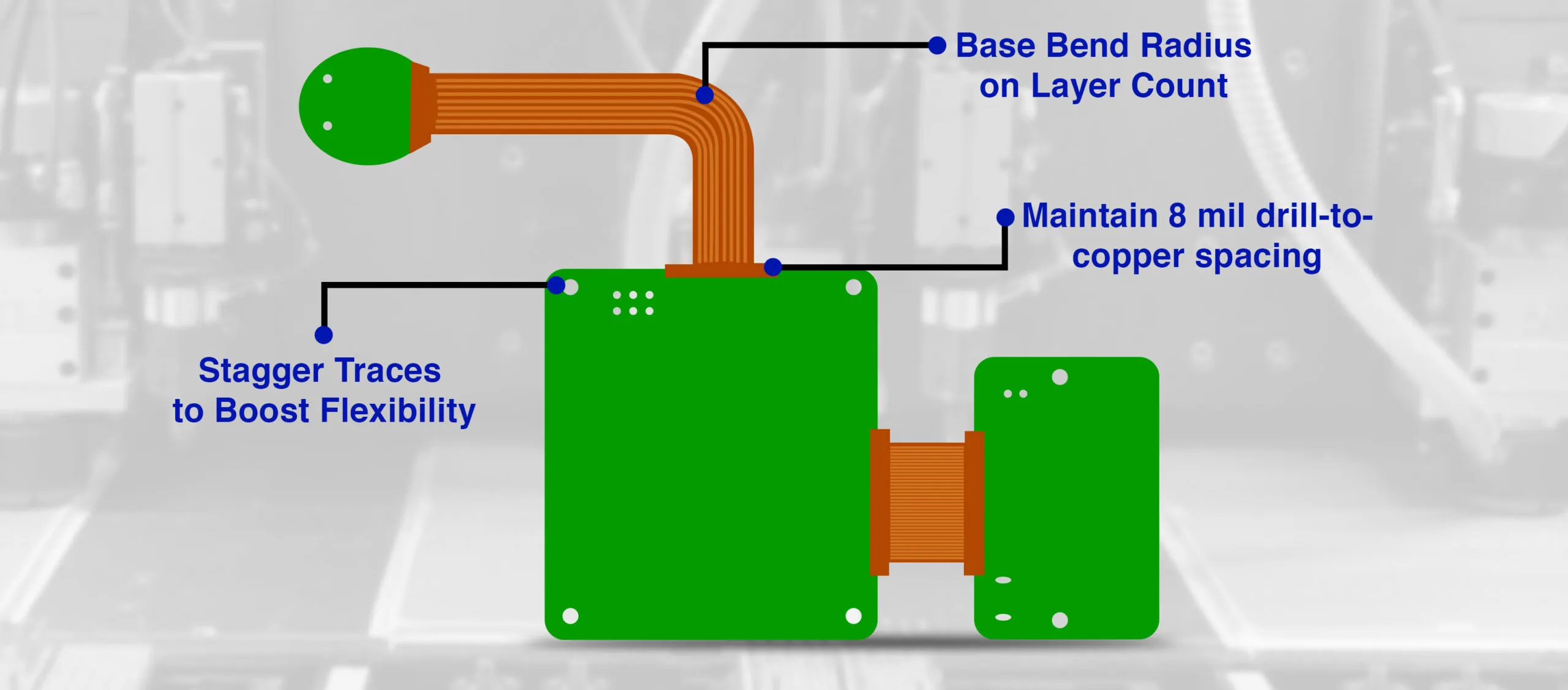
Flex PCB Bending Techniques: Ensuring Longevity
Mastering flex PCB bending techniques is crucial for applications requiring repeated motion, such as foldable devices or robotics. Poor bending design can lead to trace cracking or delamination. Consider these best practices:
- Bend Radius: Maintain a minimum bend radius of at least 6-10 times the board thickness for static bends (e.g., a 0.1 mm thick board should have a 0.6-1 mm radius). For dynamic bending, increase this to 20 times or more.
- Trace Orientation: Route traces perpendicular to the bend axis to minimize stress. Avoid placing vias or components in bend areas.
- Stiffeners: Add rigid reinforcements in non-bending areas to support components while keeping bend zones flexible.
Testing shows that designs respecting these guidelines can endure over 100,000 bending cycles without failure, critical for wearables or medical implants.
Flex PCB Adhesive Selection: Bonding for Durability
Flex PCB adhesive selection plays a vital role in maintaining structural integrity, especially under bending stress. Adhesives bond the copper foil to the substrate and attach coverlays. Key considerations include:
- Thermal Resistance: Choose adhesives that withstand reflow soldering temperatures, often exceeding 250°C.
- Flexibility: Opt for adhesives with low modulus to prevent cracking during bending. Acrylic-based adhesives are common for their balance of strength and flexibility.
- Thickness: Thinner adhesive layers (around 25 micrometers) reduce overall board stiffness, improving bendability.
Standards like IPC 4203B provide guidelines for selecting bonding materials, ensuring reliability in demanding environments like automotive or aerospace applications.
Flex PCB Connector Types: Reliable Connections in Tight Spaces
Selecting the right flex PCB connector types ensures secure electrical connections without compromising flexibility. Common options include:
- ZIF (Zero Insertion Force) Connectors: Ideal for high-density flex circuits, these connectors require minimal force to insert, reducing wear on delicate boards.
- FPC (Flexible Printed Circuit) Connectors: Designed specifically for flex PCBs, they support high-speed data transfer (up to 5 Gbps in some models) and compact designs.
- Board-to-Board Connectors: Used in rigid-flex designs, these maintain connectivity between flexible and rigid sections.
Connector placement should avoid bend zones to prevent stress. Additionally, ensure the connector’s current rating (often 0.5-1 A per contact) matches your circuit’s needs to avoid overheating.
Flex PCB Manufacturing Process: From Design to Production
Understanding the flex PCB manufacturing process helps designers create boards that are both functional and cost-effective. The process includes several stages:
- Material Preparation: Rolls of polyimide and copper foil are cut to size based on the design specifications.
- Photolithography: Circuit patterns are etched onto the copper using UV light and photoresist, achieving trace widths as narrow as 50 micrometers.
- Lamination: Layers are bonded using heat and pressure, with adhesives activated at temperatures around 180°C.
- Drilling and Plating: Vias are drilled and plated with copper to connect layers, ensuring conductivity.
- Testing: Electrical tests check for shorts or opens, while bend tests verify durability under specified conditions.
Collaboration with manufacturers early in the design phase can optimize stack-ups and reduce costs, especially for high-volume production where material waste impacts pricing.
Designing for Dynamic Bending: Challenges and Solutions
Designing for dynamic bending is one of the most complex aspects of flex PCB development. Dynamic applications, like hinges in foldable phones, require the board to withstand repeated bending without failure. Key strategies include:
- Material Fatigue Analysis: Use simulation tools to predict stress points, ensuring the design can handle cycles (often 50,000 or more) without cracking.
- Trace Design: Wider traces (e.g., 0.2 mm instead of 0.1 mm) in bend areas reduce the risk of breakage, though they increase board size.
- Bend Zone Isolation: Keep components and vias away from dynamic bend zones to minimize mechanical stress.
Testing real-world prototypes under simulated conditions (e.g., bending at 1 Hz for 24 hours) provides data on long-term reliability, helping refine designs before mass production.
Rigid-Flex PCB Design Tools: Bridging Flexibility and Stability
Rigid-flex PCB design tools cater to hybrid boards that combine rigid sections for component mounting with flexible sections for connectivity. These tools often integrate features from both rigid and flex design software, offering:
- Layer Transition Simulation: Visualize how rigid and flex layers interact, ensuring proper alignment during bending.
- Thermal and Mechanical Analysis: Assess heat dissipation (critical for power components dissipating over 1 W) and stress at rigid-flex junctions.
- Manufacturing Constraints: Built-in design rules prevent errors like overly tight bend radii at transitions.
Rigid-flex designs are common in compact devices like cameras, where space constraints demand both stability and flexibility. Tools that support impedance matching and signal integrity analysis are especially valuable for high-speed applications.
Best Practices for Designing Flexible PCBs
To wrap up, here are some overarching tips to ensure success when working with flexible and rigid-flex PCBs:
- Start with a clear understanding of the application—static or dynamic bending dictates material and design choices.
- Use simulation tools early to identify potential failure points, saving time and cost in prototyping.
- Collaborate with manufacturing partners to align your design with production capabilities, especially for complex stack-ups.
- Prioritize testing under real-world conditions to validate durability and performance metrics like signal loss (targeting less than 0.5 dB at 1 GHz for critical traces).
Conclusion: Empowering Innovation with Flexible PCB Tools
Designing for bendable electronics opens up endless possibilities for innovation, from wearable tech to advanced medical devices. By leveraging the right flexible PCB design software, selecting optimal flex PCB materials, mastering flex PCB bending techniques, and understanding the flex PCB manufacturing process, you can create reliable and cutting-edge products. Whether focusing on flex PCB adhesive selection, choosing suitable flex PCB connector types, tackling designing for dynamic bending, or using rigid-flex PCB design tools, each step contributes to a successful outcome.
At ALLPCB, we’re committed to supporting your journey in flexible PCB design with expert resources and manufacturing solutions. Dive into these tools and techniques to bring your bendable electronics to life with confidence.


