 ALLPCB


In the fast-evolving world of electronics, the demand for smaller, faster, and more efficient printed circuit boards (PCBs) has never been higher. One key innovation helping to meet these demands is via in pad technology. But what drives the adoption of this technology? Simply put, via in pad technology is used to save space, improve signal integrity, and support high-density designs, especially in high-speed digital circuits. It addresses critical needs like minimizing parasitic capacitance and inductance in high-speed digital circuits and leverages the enhanced capability of printed circuit board suppliers to fabricate smaller via diameters.
In this blog, we’ll dive deep into the reasons behind the growing use of via in pad technology. From the technical benefits for high-speed designs to advancements in fabrication techniques, we’ll explore how this approach is shaping modern PCB design and manufacturing. Let’s get started with a closer look at what via in pad technology is and why it matters.
What Is Via in Pad Technology?
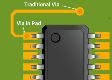
Via in pad technology refers to a PCB design technique where a via—a small conductive hole that connects different layers of a circuit board—is placed directly within the pad of a surface-mounted component. Unlike traditional vias, which are placed outside the pad and require additional space for routing, via in pad allows for a more compact layout. This method is often paired with filling the via with conductive or non-conductive material and plating it over to create a flat surface for component mounting.
This technology is especially valuable in high-density interconnect (HDI) designs, where space is limited, and performance is critical. By embedding vias within pads, designers can reduce the overall footprint of the board while maintaining or even improving electrical performance. Now, let’s explore the key factors driving the use of this technology in modern electronics.
Key Driving Factors for Via in Pad Technology
1. Space Savings for High-Density Designs
One of the primary reasons for using via in pad technology is the significant space savings it offers. As electronic devices become smaller—think smartphones, wearables, and IoT gadgets—PCBs must accommodate more components in less space. Traditional via placement often requires extra room for traces to route around vias, increasing the board’s size. Via in pad eliminates this need by placing the via directly under the component pad, freeing up valuable real estate on the board.
For example, in a typical ball grid array (BGA) package with hundreds of pins, via in pad allows designers to route connections more efficiently without expanding the board’s dimensions. This is crucial for applications where every millimeter counts. With the trend toward miniaturization showing no signs of slowing down, the ability to create compact, high-density designs is a major driver for adopting this technology.
2. Minimizing Parasitic Capacitance and Inductance in High-Speed Digital Circuits
In high-speed digital circuits, signal integrity is everything. As data rates increase—often exceeding 10 Gbps in modern applications—any interference or delay can lead to errors or performance degradation. Parasitic capacitance and inductance, which are unwanted electrical effects caused by the physical structure of the PCB, can significantly impact signal quality. Via in pad technology helps address these issues by shortening the signal path and reducing the loop area where parasitic effects occur.
For instance, in a traditional via setup, a signal traveling from a component pad to a via and then to another layer creates a longer path, increasing inductance. This can cause signal delays or crosstalk, especially at high frequencies. By placing the via directly in the pad, the signal path is minimized, reducing inductance to as low as 0.1 nH in some designs (compared to 0.5 nH or more in traditional layouts). Similarly, parasitic capacitance, which can cause signal distortion, is lowered by reducing the proximity of conductive elements.
This makes via in pad a go-to solution for applications like high-speed data communication, networking equipment, and advanced computing systems. Designers working on circuits with tight timing requirements or high-frequency signals rely on this technology to maintain performance and reliability.
3. Enhanced Capability of PCB Suppliers to Fabricate Smaller Via Diameters
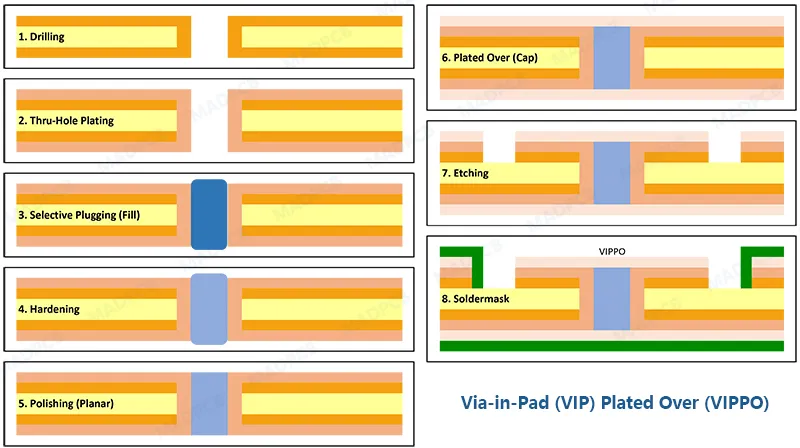
Another critical factor driving the use of via in pad technology is the advancements in PCB manufacturing capabilities. Modern fabrication techniques have made it possible to create smaller via diameters, often as tiny as 0.1 mm or less, with high precision. This is a game-changer for via in pad designs, as smaller vias can fit within the tight constraints of component pads without compromising structural integrity or electrical performance.
In the past, larger via sizes—typically 0.3 mm or more—made it challenging to place vias directly under pads, especially for fine-pitch components. However, with the rise of laser drilling and advanced plating processes, manufacturers can now produce microvias with diameters small enough to support via in pad layouts. This capability not only enables more compact designs but also ensures reliable connections between layers, even in multilayer boards with complex routing.
At ALLPCB, we’ve seen firsthand how these manufacturing advancements empower designers to push the boundaries of what’s possible. Smaller via diameters mean more flexibility in layout design, making via in pad a practical choice for cutting-edge projects.
4. Improved Thermal Management
Thermal management is a growing concern in modern electronics, especially as components become more powerful and densely packed. Via in pad technology can play a role in dissipating heat more effectively. By placing vias directly under components that generate significant heat, such as processors or power ICs, the vias can act as thermal conduits, transferring heat to other layers or heat sinks within the PCB.
For example, in a design with a high-power BGA component, multiple vias in pad can be used to create a thermal pathway, reducing the component’s operating temperature by several degrees Celsius. This not only enhances the reliability of the device but also extends its lifespan. As thermal challenges continue to grow in industries like automotive and aerospace, via in pad offers a practical solution for managing heat without adding bulk to the design.
5. Support for Fine-Pitch Components
The rise of fine-pitch components, such as BGAs and quad flat no-lead (QFN) packages with pin spacing as small as 0.4 mm, has made traditional via placement increasingly impractical. Routing traces between tightly spaced pins often requires more board space, which isn’t always available in compact designs. Via in pad technology solves this problem by allowing vias to be placed directly under the pads of these components, simplifying routing and reducing the need for additional layers.
This is particularly important in applications like mobile devices and high-performance computing, where fine-pitch components are the norm. By supporting these components, via in pad technology enables designers to create smaller, more efficient boards without sacrificing functionality.
Challenges and Considerations in Via in Pad Technology
While via in pad technology offers numerous benefits, it’s not without challenges. Understanding these hurdles is essential for designers and engineers looking to implement this approach in their projects.
Manufacturing Complexity
Creating vias within pads requires advanced manufacturing techniques, such as precise drilling and via filling. If not done correctly, issues like voiding (air pockets in the via fill) or uneven plating can occur, leading to reliability problems. Working with a trusted PCB supplier who has experience with via in pad fabrication is crucial to avoid these pitfalls.
Cost Considerations
Due to the added complexity, via in pad designs can be more expensive to produce than traditional layouts. The use of microvias, via filling, and additional process steps can increase costs, especially for high-volume production. However, the benefits of space savings and improved performance often outweigh the added expense, particularly in high-end applications.
Design Constraints
Designers must also consider the impact of via in pad on assembly processes. For instance, during soldering, there’s a risk of solder wicking into the via if it’s not properly filled or capped, which can lead to poor connections. Careful design and coordination with the manufacturer can mitigate these risks.
How Via in Pad Technology Shapes the Future of PCB Design
As the electronics industry continues to push toward smaller, faster, and more efficient devices, via in pad technology will play an increasingly important role. The need to minimize parasitic capacitance and inductance in high-speed digital circuits ensures that this technology remains a top choice for cutting-edge applications. Meanwhile, the enhanced capability of printed circuit board suppliers to fabricate smaller via diameters means that via in pad designs are more accessible than ever before.
From 5G infrastructure to advanced medical devices, the applications for via in pad are vast and growing. Designers who embrace this technology can create boards that meet the stringent demands of modern electronics while staying ahead of the curve in terms of performance and reliability.
Conclusion
Via in pad technology is transforming the way PCBs are designed and manufactured, driven by the need for compact layouts, improved signal integrity, and support for high-speed digital circuits. By minimizing parasitic capacitance and inductance, leveraging smaller via diameters, and addressing thermal challenges, this technology meets the demands of modern electronics head-on. While there are challenges to consider, the benefits make via in pad a powerful tool for engineers and designers.
As advancements in fabrication continue to evolve, via in pad will only become more integral to the future of PCB design. Whether you’re tackling a complex high-density project or optimizing for high-frequency performance, understanding and utilizing this technology can give you a competitive edge in the fast-paced world of electronics.


