 ALLPCB


If you're facing issues like solder bridging, solder balls, insufficient solder, solder paste slump, misalignment, or stencil clogging during PCB assembly, you're not alone. These common solder paste application defects can disrupt production and affect the quality of your boards. In this comprehensive guide, we'll dive deep into identifying these problems, understanding their causes, and providing actionable solutions to help you achieve flawless solder paste application. Whether you're a seasoned engineer or new to surface mount technology (SMT), this blog will equip you with the tools to troubleshoot effectively and improve your manufacturing process.
Why Solder Paste Application Matters in PCB Assembly
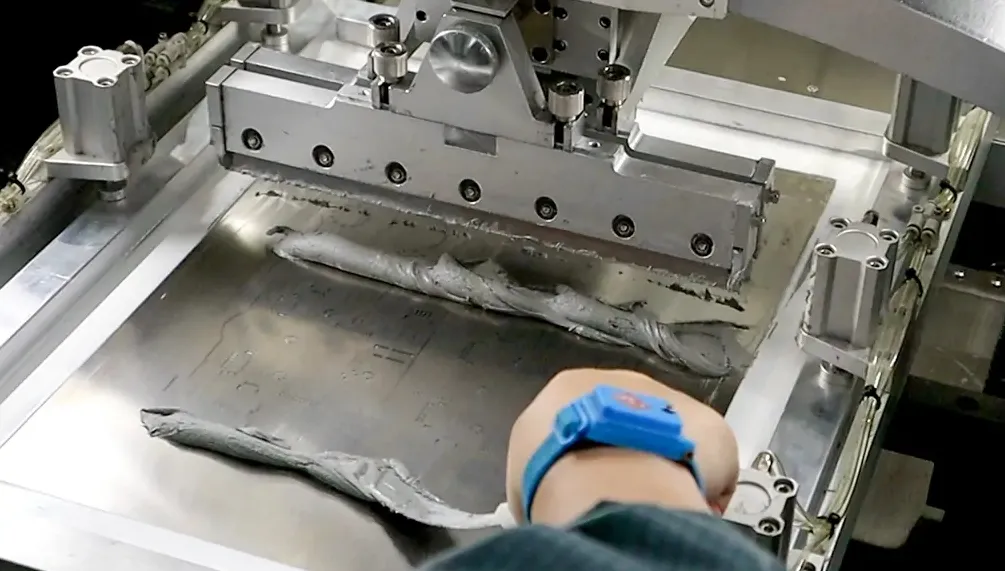
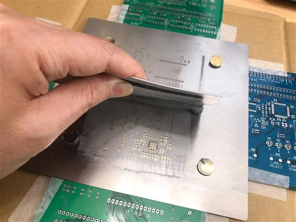
Solder paste application is a critical step in the SMT process, where components are mounted directly onto the surface of a printed circuit board (PCB). The paste, a mixture of tiny solder particles and flux, acts as the adhesive and conductive material that forms reliable electrical connections during reflow soldering. However, even minor errors in application can lead to defects that compromise the functionality and reliability of the final product. By understanding and addressing issues like solder bridging or stencil clogging, you can minimize rework, reduce costs, and ensure high-quality assemblies.
Common Solder Paste Application Defects and Their Causes
Let’s break down the most frequent solder paste application defects, their root causes, and how they impact the assembly process. Each defect can often be traced back to specific variables like stencil design, paste properties, or equipment settings.
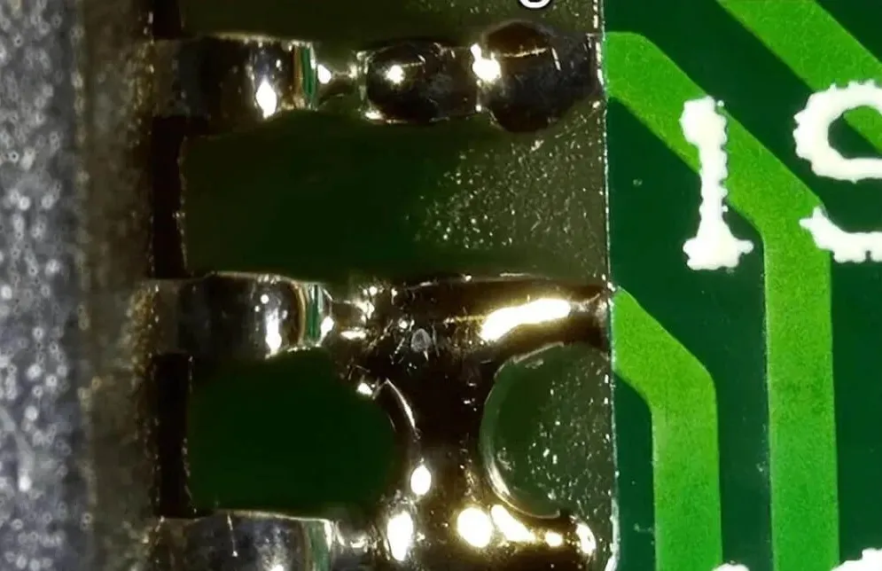
1. Solder Bridging: Unwanted Connections Between Pads
Solder bridging occurs when excess solder paste creates an unintended connection between two or more adjacent pads or leads, resulting in a short circuit. This defect is particularly common in fine-pitch components where pads are closely spaced, sometimes as little as 0.4mm apart.
Causes:
- Excessive solder paste volume due to oversized stencil apertures.
- Poor stencil alignment, causing paste to spread beyond intended areas.
- Inadequate separation between pads in the PCB design.
- High humidity or improper paste storage leading to increased viscosity and poor flow control.
Impact: Solder bridging can cause electrical shorts, leading to circuit failure or unreliable performance. In high-density designs, detecting and repairing bridges can be time-consuming and costly.
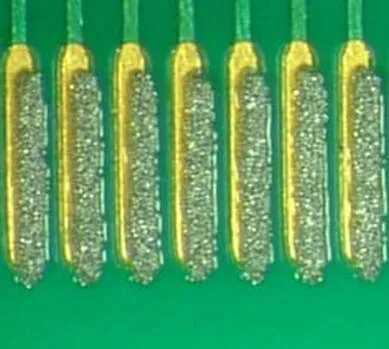
2. Solder Balls: Small Spheres of Unattached Solder
Solder balls are tiny, spherical beads of solder that form on or around the PCB surface during reflow. They often appear as isolated defects that don't connect to any pad or component lead.
Causes:
- Excess moisture in the solder paste or PCB, causing spattering during reflow.
- Inconsistent stencil printing pressure, leading to uneven paste deposits.
- Improper reflow profile with rapid temperature changes that cause paste to splatter.
- Oxidation of solder particles due to prolonged exposure to air before reflow.
Impact: Solder balls can create unintended electrical connections if they move during operation, posing a risk of shorts or intermittent failures, especially in high-reliability applications like automotive or medical devices.
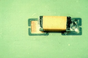
3. Insufficient Solder: Weak or Missing Joints
Insufficient solder happens when there isn’t enough paste applied to form a proper joint between the component lead and the pad. This often results in weak or incomplete connections.
Causes:
- Undersized stencil apertures, restricting the amount of paste deposited.
- Worn-out or damaged stencils that fail to transfer paste effectively.
- Incorrect squeegee pressure or angle during printing, leading to incomplete paste release.
- Solder paste degradation due to expired shelf life or improper storage.
Impact: Weak solder joints can lead to mechanical failure under stress or thermal cycling, causing components to detach or circuits to fail. For example, a joint with only 50% of the required solder volume may crack after just a few thermal cycles.
4. Solder Paste Slump: Loss of Shape After Printing
Solder paste slump refers to the spreading or collapse of paste deposits after printing, often resulting in blurred or merged shapes that deviate from the intended stencil pattern.
Causes:
- Low viscosity of solder paste due to high temperature or humidity in the printing environment.
- Excessive paste volume applied through oversized apertures or high squeegee pressure.
- Delayed reflow after printing, allowing paste to settle and spread over time.
- Poor stencil-to-board contact, causing uneven paste release.
Impact: Slumping can lead to solder bridging or insufficient solder in critical areas, as the paste may not stay in place to form proper joints during reflow.
5. Misalignment: Paste or Components Out of Position
Misalignment occurs when solder paste is not deposited accurately on the pads or when components shift during placement or reflow, leading to poor connections.
Causes:
- Inaccurate stencil alignment with the PCB during printing.
- Vibration or movement during component placement, especially with high-speed pick-and-place machines.
- Inconsistent PCB flatness or warpage, affecting contact with the stencil.
- Improper reflow profile causing components to shift due to uneven heating.
Impact: Misaligned paste or components can result in open circuits or weak joints, requiring manual rework. In severe cases, it may render the board unusable.
6. Stencil Clogging: Blocked Apertures Preventing Paste Transfer
Stencil clogging happens when solder paste or debris blocks the apertures of the stencil, preventing proper paste deposition on the PCB.
Causes:
- Insufficient cleaning of the stencil between prints, allowing paste residue to harden.
- Use of low-quality or degraded solder paste with inconsistent particle size.
- Small aperture sizes (e.g., below 0.2mm) that are prone to blockage, especially in fine-pitch designs.
- Improper storage of paste, leading to drying or clumping.
Impact: Clogged stencils result in incomplete or missing paste deposits, leading to insufficient solder and potential open circuits after reflow.
Practical Solutions for Troubleshooting Solder Paste Defects
Now that we’ve identified the common defects and their causes, let’s explore actionable solutions to troubleshoot and prevent these issues. Implementing these strategies can significantly improve your SMT process yield.
Solving Solder Bridging
- Optimize Stencil Design: Ensure aperture sizes are appropriate for pad dimensions, typically with a 10-20% reduction in area for fine-pitch components to control paste volume.
- Improve Alignment: Use vision systems or fiducial marks to align the stencil precisely with the PCB.
- Control Environment: Maintain a printing environment with humidity below 60% and temperature between 20-25°C to prevent paste from becoming too fluid.
- Adjust Reflow Profile: Ensure a gradual ramp-up in temperature (1-3°C per second) to avoid paste spreading during heating.
Preventing Solder Balls
- Store Materials Properly: Keep solder paste refrigerated at 2-10°C and allow it to reach room temperature before use to avoid moisture condensation.
- Use Correct Reflow Profile: Avoid rapid temperature spikes; aim for a preheat stage of 120-150°C for 60-90 seconds to evaporate moisture slowly.
- Check Printing Parameters: Maintain consistent squeegee pressure (typically 8-12 kg for a 300mm blade) to ensure even paste deposition.
- Inspect PCB Condition: Use boards within 24 hours of baking to minimize moisture absorption.
Addressing Insufficient Solder
- Verify Stencil Apertures: Check for wear or damage in the stencil; apertures should match pad sizes with a tolerance of ±5%.
- Optimize Printing Settings: Adjust squeegee pressure and speed (e.g., 20-40 mm/s) to ensure complete paste transfer.
- Use Fresh Paste: Monitor the expiration date of solder paste and avoid using material beyond 6 months of manufacture, even if stored correctly.
- Inspect Equipment: Regularly calibrate printing machines to maintain consistent performance.
Fixing Solder Paste Slump
- Control Paste Properties: Use paste with appropriate viscosity (typically 800-1000 kcps for Type 3 paste) and store it under recommended conditions.
- Minimize Delay: Proceed to reflow within 1-2 hours after printing to prevent paste from settling.
- Adjust Printing Environment: Keep ambient temperature below 25°C and avoid high humidity to maintain paste integrity.
- Check Stencil Contact: Ensure the stencil is flush with the PCB using proper fixturing or support pins.
Correcting Misalignment
- Enhance Alignment Systems: Use automated optical inspection (AOI) or camera systems to verify stencil and component placement accuracy.
- Stabilize Equipment: Minimize vibrations in pick-and-place machines by securing them on stable surfaces and performing regular maintenance.
- Address PCB Warpage: Store PCBs flat and use vacuum or edge supports during printing to maintain flatness.
- Optimize Reflow: Use a balanced reflow profile with uniform heating to prevent component shift.
Eliminating Stencil Clogging
- Regular Cleaning: Clean stencils after every 5-10 prints using isopropyl alcohol or specialized stencil cleaners to remove residue.
- Use Quality Paste: Select solder paste with consistent particle size distribution (e.g., Type 3 or 4 for fine-pitch applications).
- Optimize Aperture Design: For small apertures, consider tapered designs with a wider opening on the squeegee side to facilitate paste release.
- Monitor Storage: Avoid exposing paste to air for extended periods; reseal containers immediately after use.
Best Practices for Consistent Solder Paste Application
Beyond troubleshooting specific defects, adopting best practices can prevent issues from arising in the first place. Here are key strategies to ensure consistent results:
- Invest in Solder Paste Inspection (SPI): Use SPI systems to measure paste volume and alignment after printing. For instance, aim for a paste height of 100-150 microns for standard applications to ensure adequate solder volume.
- Maintain Equipment: Regularly service printers and reflow ovens to avoid mechanical issues that contribute to defects.
- Train Operators: Ensure staff are trained in proper paste handling, stencil setup, and equipment operation to minimize human error.
- Document Processes: Keep detailed records of printing parameters, reflow profiles, and defect rates to identify patterns and areas for improvement.
Conclusion: Mastering Solder Paste Application for Flawless PCBs
Troubleshooting common solder paste application defects like solder bridging, solder balls, insufficient solder, solder paste slump, misalignment, and stencil clogging is essential for achieving high-quality PCB assemblies. By understanding the root causes of these issues and implementing the practical solutions outlined in this guide, you can significantly reduce defects, improve yield, and ensure reliable performance in your electronic products. At ALLPCB, we’re committed to supporting your manufacturing journey with resources and expertise to tackle challenges like these. With the right approach and attention to detail, flawless solder paste application is within your reach.


