 ALLPCB


Wave soldering is a critical process in PCB assembly, allowing for fast and efficient soldering of through-hole components. However, defects during wave soldering can lead to costly rework, reduced reliability, and frustrated engineers. If you're searching for solutions to common wave soldering issues like solder bridging, insufficient solder, solder balling, or lifted components, you've come to the right place. In this comprehensive guide, we'll help you identify these defects, understand their root causes, and implement practical prevention strategies to ensure high-quality PCB assemblies.
Whether you're a seasoned engineer or new to PCB manufacturing, this ultimate guide dives deep into the most common wave soldering defects. We'll explore specific problems such as wave soldering defects solder bridging, wave soldering defects insufficient solder, wave soldering defects solder balling, and wave soldering defects lifted components. By the end, you'll have actionable insights to optimize your wave soldering process and minimize defects. Let's get started!
What Is Wave Soldering and Why Does It Matter?
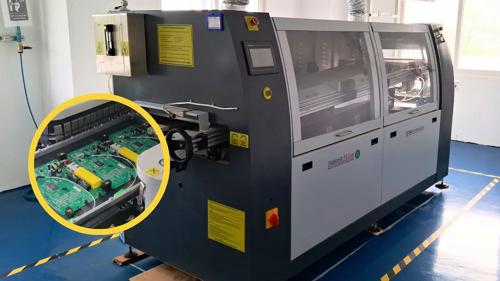
Wave soldering is a bulk soldering technique used in PCB assembly to solder through-hole components to a circuit board. The process involves passing the PCB over a molten solder wave, which creates reliable electrical connections between components and the board. This method is highly efficient for large-scale production, often reducing assembly time by up to 50% compared to manual soldering.
However, the wave soldering process is prone to defects if not carefully controlled. These defects can compromise the functionality of the PCB, leading to failures in the final product. Understanding and preventing issues like solder bridging or insufficient solder is essential for maintaining quality and reliability in electronics manufacturing.
Common Wave Soldering Defects: An Overview
Before diving into specific defects, it's important to recognize that wave soldering defects often stem from a combination of factors, including improper temperature settings, flux application issues, or PCB design flaws. The defect rate in wave soldering can be as high as 50% in poorly optimized processes, making defect identification and prevention a top priority. Below, we’ll cover the four most common wave soldering defects in detail, focusing on identification, causes, and prevention.
1. Wave Soldering Defects: Solder Bridging
What Is Solder Bridging?
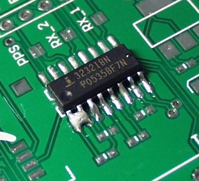
Solder bridging occurs when excess solder creates an unintended connection between two or more adjacent pads or leads on a PCB. This defect can cause short circuits, leading to malfunctioning electronics. Solder bridges are often visible as small blobs of solder connecting areas that should remain separate.
Causes of Solder Bridging
- Excessive Solder: If the solder wave is too high or the PCB lingers in the wave for too long, excess solder can accumulate and form bridges.
- Improper Pad Spacing: PCB designs with pads or leads placed too closely together increase the risk of bridging, especially if spacing is less than 0.1 inches (2.54 mm).
- Inadequate Flux Application: Flux helps solder flow properly, but insufficient or uneven flux can cause solder to stick in unwanted areas.
- High Solder Temperature: Temperatures above the recommended range (typically 250-260°C for lead-free solder) can make solder too fluid, increasing the likelihood of bridging.
Prevention Tips for Solder Bridging
- Optimize the height and speed of the solder wave to minimize excess solder exposure. A conveyor speed of 1.5-2.5 meters per minute is often ideal for most setups.
- Ensure proper PCB design by maintaining adequate spacing between pads and leads. Use design software to check for spacing issues before manufacturing.
- Apply flux evenly and in the correct amount. Use automated fluxing systems for consistent results.
- Monitor and control solder pot temperature to stay within the manufacturer’s recommended range.
2. Wave Soldering Defects: Insufficient Solder
What Is Insufficient Solder?
Insufficient solder refers to a lack of solder on component leads or pads, resulting in weak or incomplete joints. This defect can lead to poor electrical connections and mechanical failures, especially under stress or vibration. You might notice joints that appear dull or incomplete during inspection.
Causes of Insufficient Solder
- Inadequate Preheat: If the PCB and components are not preheated sufficiently (typically to 100-120°C), the solder may not wet properly, leading to incomplete joints.
- Low Solder Wave Height: A wave that’s too low may not fully contact all leads, especially on larger components.
- Contaminated Solder or Leads: Oxidation or debris on component leads or in the solder pot can prevent proper adhesion.
- Improper Fluxing: Without enough flux, solder may not flow evenly across all areas, resulting in insufficient coverage.
Prevention Tips for Insufficient Solder
- Set preheat temperatures to ensure the PCB reaches the ideal range before entering the solder wave. Monitor with thermal profiling tools for accuracy.
- Adjust the solder wave height to ensure full contact with all component leads. Test with a sample board to confirm coverage.
- Regularly clean and maintain the solder pot to remove dross and contaminants. Use high-purity solder to minimize issues.
- Ensure consistent flux application by checking spray or foam fluxer settings before each run.
3. Wave Soldering Defects: Solder Balling
What Is Solder Balling?
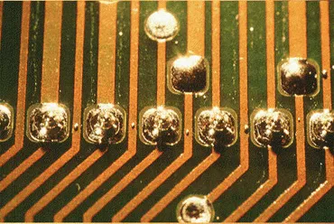
Solder balling occurs when small, spherical beads of solder form on the PCB surface instead of adhering to the intended areas. These balls can roll around, potentially causing short circuits or other reliability issues. Solder balls are often visible during post-soldering inspection as tiny, scattered dots.
Causes of Solder Balling
- Excessive Moisture: Moisture trapped in the PCB or components can vaporize during soldering, causing solder to splatter and form balls.
- High Solder Temperature: If the solder pot exceeds optimal temperatures (above 260°C for lead-free solder), it can cause spattering.
- Improper Flux Activation: If flux isn’t activated properly due to low preheat temperatures, it can lead to uneven solder flow and balling.
- Turbulent Solder Wave: A poorly adjusted wave can create turbulence, splashing solder droplets onto the board.
Prevention Tips for Solder Balling
- Bake PCBs and components before soldering to remove moisture, especially if they’ve been stored in humid conditions. A baking process at 100°C for 2-4 hours is often sufficient.
- Keep solder temperatures within the recommended range and monitor with a calibrated thermometer.
- Optimize preheat settings to ensure flux activation, typically between 100-120°C for most assemblies.
- Adjust the solder wave to minimize turbulence, using a smooth, laminar flow for best results.
Related Reading: Optimizing Wave Soldering Temperature: A Key Factor for Reliable PCB Joints
4. Wave Soldering Defects: Lifted Components
What Are Lifted Components?
Lifted components occur when a component is partially or completely detached from the PCB during or after wave soldering. This defect compromises the mechanical and electrical integrity of the assembly, often requiring rework. You might notice components that are tilted or completely separated from their pads.
Causes of Lifted Components
- Thermal Shock: Rapid temperature changes during soldering can cause components to lift due to uneven expansion. For instance, a temperature delta of over 100°C between preheat and solder wave can be problematic.
- Poor Component Placement: If components are not securely placed or glued before soldering, the force of the solder wave can dislodge them.
- Insufficient Flux: Without proper flux, solder may not wet the pads evenly, leading to weak adhesion and component lifting.
- Incorrect Wave Angle: A wave angle that’s too steep can exert excessive force on components, pushing them off the board.
Prevention Tips for Lifted Components
- Use a gradual preheat to minimize thermal shock, ensuring a temperature ramp rate of no more than 2-3°C per second.
- Secure components with adhesive or proper insertion techniques before wave soldering to withstand the wave’s force.
- Apply adequate flux to promote strong solder wetting and adhesion to pads.
- Adjust the solder wave angle to a gentler slope, typically around 7-10 degrees, to reduce impact on components.
General Best Practices for Preventing Wave Soldering Defects
Beyond addressing specific defects, adopting a proactive approach to your wave soldering process can significantly reduce overall issues. Here are some best practices to ensure consistent, high-quality results:
- Regular Maintenance: Clean and maintain wave soldering equipment regularly to prevent contamination and ensure consistent performance. Check solder pot dross levels daily and remove impurities.
- Thermal Profiling: Use thermal profiling tools to monitor preheat and solder wave temperatures across the PCB. Aim for a peak temperature of 250-260°C for lead-free solder and ensure even heating.
- Quality Materials: Use high-quality solder, flux, and components to minimize defects caused by material inconsistencies. Verify material specifications with suppliers.
- Operator Training: Train operators to recognize early signs of defects and adjust machine settings as needed. A well-trained team can reduce defect rates by up to 30%.
- PCB Design Optimization: Design PCBs with wave soldering in mind, ensuring proper pad spacing, component orientation, and thermal relief to avoid issues like bridging or insufficient solder.
How to Inspect and Repair Wave Soldering Defects
Even with the best prevention strategies, some defects may still occur. Implementing a robust inspection and repair process can help catch issues early and maintain quality.
Inspection Techniques
- Visual Inspection: Use magnifying tools or automated optical inspection (AOI) systems to check for visible defects like solder bridging or lifted components. AOI systems can detect up to 95% of surface defects.
- X-Ray Inspection: For hidden joints or internal defects, X-ray systems can reveal issues like insufficient solder in through-hole connections.
- Functional Testing: Test the PCB for electrical continuity and performance to identify defects that may not be visible, such as weak joints.
Repair Methods
- For solder bridging, use a desoldering braid or suction tool to remove excess solder, then clean the area with isopropyl alcohol.
- For insufficient solder, manually apply solder to the affected joint using a soldering iron with a fine tip, ensuring proper wetting.
- For solder balling, carefully remove loose balls with a brush or compressed air, then inspect for potential short circuits.
- For lifted components, reposition and secure the component, then resolder the joint with fresh solder and flux.
Related Reading: Troubleshooting Common Wave Soldering Problems: A Practical Guide for Engineers
Conclusion: Mastering Wave Soldering for Flawless PCBs
Wave soldering is a powerful technique for efficient PCB assembly, but it comes with challenges that can lead to defects like solder bridging, insufficient solder, solder balling, and lifted components. By understanding the causes of these issues—such as improper temperatures, inadequate flux, or poor PCB design—you can take targeted steps to prevent them. From optimizing machine settings to maintaining high-quality materials, the strategies outlined in this guide will help you tackle wave soldering defects solder bridging, wave soldering defects insufficient solder, wave soldering defects solder balling, and wave soldering defects lifted components with confidence.
Implementing regular maintenance, thorough inspections, and best practices can drastically reduce defect rates, saving time and resources in your manufacturing process. With the right approach, you’ll achieve reliable, high-quality PCB assemblies every time. Keep this guide handy as a reference for troubleshooting and optimizing your wave soldering process, and watch your production quality soar!


