 ALLPCB


In the world of electronics manufacturing, efficiency and precision are everything. If you're looking to streamline your Surface Mount Technology (SMT) assembly process, one of the most critical factors to consider is PCB panel size optimization. Properly designed panels can save time, reduce costs, and improve the quality of your final product. So, how do you optimize PCB panel size for SMT assembly? The answer lies in balancing design requirements with manufacturing capabilities, ensuring compatibility with automated assembly equipment, and minimizing material waste.
In this comprehensive guide, we'll walk you through everything you need to know about PCB panel size for SMT assembly, from the basics of panelization to advanced tips for optimizing your designs for automated pick-and-place machines and reflow soldering. Whether you're a seasoned engineer or new to PCB design, this guide will provide actionable insights to enhance your production process.
What Is PCB Panelization and Why Does It Matter for SMT Assembly?
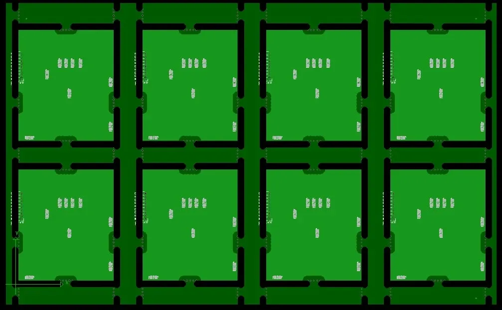
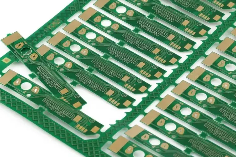
PCB panelization is the process of grouping multiple individual printed circuit boards (PCBs) into a single larger panel or array. This panel is then used during manufacturing and assembly, allowing multiple boards to be processed at once. For SMT assembly, where components are placed and soldered onto the board's surface using automated equipment, panelization is a game-changer. It enables high-volume production by reducing handling time and ensuring consistent quality across batches.
Optimizing PCB panel size for SMT assembly is crucial because it directly impacts manufacturing efficiency. A well-designed panel ensures that automated machines, like pick-and-place systems, can operate at maximum speed without errors. It also minimizes material waste, which can lower production costs. For instance, a poorly sized panel might lead to excessive unused space, increasing the cost per board, or it might not fit properly on assembly equipment, causing delays.
Key Factors in PCB Panel Size Optimization for SMT Assembly
When designing a panel for SMT assembly, several factors come into play. Below, we break down the most important considerations to help you achieve the best results.
1. Equipment Compatibility for Automated Assembly
One of the first things to consider when optimizing PCB panel size for SMT assembly is the specifications of your manufacturing equipment. Automated assembly machines, such as pick-and-place systems, have specific size limitations for the panels they can handle. Most standard SMT equipment can process panels ranging from 50mm x 50mm to 510mm x 460mm, though these dimensions vary based on the machine model and manufacturer.
To avoid production hiccups, always check the maximum and minimum panel sizes supported by your assembly line. If your panel is too large, it may not fit into the machine, while a panel that's too small could lead to inefficient processing or handling errors. Coordinate with your manufacturing partner to confirm these details early in the design phase.
2. Board Spacing and Edge Clearance
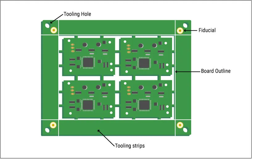
Spacing between individual boards on a panel, as well as clearance from the panel edges, is another critical aspect of PCB panelization for automated assembly. Proper spacing ensures that automated tools can access each board without interference. A common guideline is to maintain at least 5mm of spacing between boards and a 10mm clearance from the panel edges to accommodate tooling rails or fiducial marks used by SMT machines for alignment.
Insufficient spacing can lead to issues during the depanelization process (separating individual boards after assembly) or cause damage to components near the edges. On the other hand, too much spacing wastes valuable panel space, driving up costs.
3. Panel Size for Pick-and-Place Efficiency
Optimizing PCB panel for pick-and-place machines is all about maximizing throughput. Pick-and-place machines work best when they can place components on multiple boards in a single cycle without frequent repositioning. A panel size that aligns with the machine's working area can significantly reduce assembly time.
For example, if your pick-and-place machine has a working area of 400mm x 300mm, design your panel to fit within these dimensions while including as many individual boards as possible. This reduces the number of panel changes during production, saving time and minimizing the risk of human error during setup.
4. Considerations for Reflow Soldering
PCB panel size for reflow soldering also plays a role in achieving consistent results. Reflow ovens heat the panel to melt solder paste and secure components to the board. If the panel size is not optimized, uneven heat distribution can occur, leading to soldering defects like tombstoning or insufficient solder joints.
To avoid these issues, ensure that your panel size matches the reflow oven's conveyor width, typically between 300mm and 500mm for standard equipment. Additionally, maintain uniform board density across the panel to promote even heating. Large empty spaces or uneven board layouts can cause thermal imbalances, affecting soldering quality.
Standard PCB Panel Sizes for SMT Assembly
While panel sizes can vary based on specific project needs, there are industry-standard dimensions that most manufacturers follow for SMT assembly. These standards help ensure compatibility with automated equipment and streamline production.
- Small Panels: Often around 100mm x 100mm, used for prototyping or small-batch production. These are ideal when testing designs before scaling up.
- Medium Panels: Typically 200mm x 300mm, suitable for mid-volume runs and compatible with most SMT equipment.
- Large Panels: Up to 500mm x 400mm or more, used for high-volume production to maximize efficiency and reduce handling time.
Choosing the right panel size depends on your production volume and the capabilities of your assembly partner. For instance, a medium panel might be perfect for a run of 1,000 units, while a large panel could be more cost-effective for 10,000 units or more.
Best Practices for SMT Assembly Panel Design
Designing a panel for SMT assembly goes beyond just picking the right size. Here are some best practices to ensure your PCB panelization for automated assembly leads to smooth production and high-quality results.
1. Use Fiducial Marks for Alignment
Fiducial marks are small reference points on the panel that help automated machines align components accurately. Place at least three fiducial marks on the panel, ideally near the corners, to ensure precise positioning during SMT assembly. Each mark should be a small copper dot (about 1mm in diameter) with a clear surrounding area free of solder mask.
2. Incorporate Tooling Holes and Rails
Tooling holes and rails are essential for securing the panel during assembly. Most SMT equipment requires tooling holes with a diameter of 3mm to 4mm, placed along the panel edges. Rails, or extra material along the edges, provide additional stability and help the panel move smoothly through the assembly line.
3. Balance Board Orientation
When arranging individual boards on a panel, consider their orientation. Aligning boards in the same direction can simplify component placement and reduce machine setup time. However, for boards with unique shapes, you might need to rotate some to maximize panel space utilization. Use PCB design software to experiment with layouts and find the most efficient arrangement.
4. Plan for Depanelization
After assembly, individual boards must be separated from the panel through a process called depanelization. Design your panel with this step in mind by including breakaway tabs or V-grooves between boards. Breakaway tabs are small, perforated connections that allow easy manual separation, while V-grooves enable machine cutting with minimal stress on components. Ensure that these features are placed away from sensitive areas to avoid damage.
Benefits of Optimizing PCB Panel Size for SMT Assembly
Investing time in optimizing your PCB panel size offers several advantages that can significantly impact your bottom line and product quality.
- Cost Reduction: Efficient panel designs minimize material waste, reducing the cost per board. For high-volume runs, even a 5% reduction in waste can lead to substantial savings.
- Faster Production: Panels that are compatible with automated equipment reduce setup and processing times, allowing for quicker turnaround.
- Improved Quality: Proper panel design ensures consistent assembly and soldering, leading to fewer defects and higher reliability.
- Scalability: Optimized panels make it easier to scale production from prototypes to full runs without major design changes.
Common Mistakes to Avoid in PCB Panelization for Automated Assembly
Even experienced designers can make mistakes when panelizing PCBs for SMT assembly. Here are some pitfalls to watch out for:
- Ignoring Equipment Limitations: Failing to account for the size constraints of SMT machines can halt production. Always verify equipment specs before finalizing your panel design.
- Overcrowding Boards: Placing too many boards on a panel without proper spacing can lead to assembly errors or damage during depanelization.
- Neglecting Thermal Balance: Uneven board layouts can cause thermal issues during reflow soldering, resulting in defective solder joints.
- Skipping Fiducial Marks: Without proper alignment markers, automated machines may misplace components, leading to costly rework.
How to Collaborate with Your Manufacturing Partner for Optimal Results
Effective communication with your manufacturing partner is key to successful PCB panelization. Share your design files early and discuss specific requirements, such as panel size, spacing, and depanelization methods. Many PCB manufacturers offer design guidelines tailored to their equipment, which can help you avoid common issues.
Additionally, request a panel layout review before production begins. This step allows you to catch potential problems, like insufficient edge clearance or incompatible panel dimensions, before they impact your project timeline.
Conclusion: Mastering PCB Panel Size Optimization for SMT Assembly
Optimizing PCB panel size for SMT assembly is a critical step in achieving efficient, cost-effective, and high-quality electronics manufacturing. By carefully considering factors like equipment compatibility, spacing, and thermal balance, you can design panels that streamline automated assembly processes and reduce production costs. Implementing best practices, such as using fiducial marks and planning for depanelization, further enhances the success of your project.
Whether you're focusing on PCB panel size for reflow soldering or optimizing PCB panel for pick-and-place machines, the principles outlined in this guide will help you navigate the complexities of panelization. With the right approach, you can transform your PCB designs into a seamless part of the SMT assembly process, ensuring better outcomes for your products.
Start applying these strategies to your next project and experience the difference that optimized panel design can make in your production workflow.


