 ALLPCB


In the world of PCB assembly, achieving high-quality solder joints is crucial for ensuring the reliability and performance of electronic devices. One often-overlooked factor that significantly affects solder joint quality is stencil thickness. But how exactly does stencil thickness impact solder joint quality? In short, stencil thickness determines the volume of solder paste deposited on the PCB pads, which directly influences the strength, reliability, and electrical connection of the solder joint. Too much or too little solder paste due to improper stencil thickness can lead to defects like bridging, insufficient solder, or poor mechanical bonding.
In this comprehensive guide, we’ll dive deep into the relationship between stencil thickness, solder paste volume, and solder joint quality. We’ll explore the key stencil printing parameters, their effects on PCB assembly quality, and provide actionable insights for optimizing your assembly process. Whether you’re an engineer or a manufacturer, this blog will equip you with the knowledge to improve your soldering outcomes.
Understanding Stencil Thickness in PCB Assembly
Stencil thickness refers to the depth of the metal sheet (usually stainless steel) used in the stencil printing process during PCB assembly. This sheet contains precisely cut apertures that align with the pads on a printed circuit board (PCB). During printing, solder paste is pushed through these apertures onto the pads, where components will later be placed and soldered.
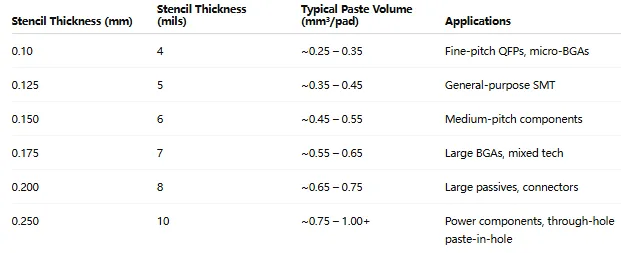
The thickness of the stencil directly controls the amount of solder paste deposited. Common stencil thicknesses range from 0.08 mm to 0.15 mm, depending on the components and design requirements. For instance, finer-pitch components like 0201 chips often require thinner stencils (around 0.10 mm) to avoid excessive paste, while larger components might need thicker stencils (up to 0.15 mm) for sufficient solder volume.
Why Solder Joint Quality Matters
Solder joints are the critical connections between electronic components and the PCB. They provide both electrical conductivity and mechanical strength. Poor solder joint quality can lead to issues like:
- Electrical Failures: Insufficient solder can cause open circuits, while excess solder may lead to shorts or bridging between pads.
- Mechanical Weakness: Weak joints can crack or break under thermal or mechanical stress, leading to device failure.
- Reliability Issues: Inconsistent solder joints can fail over time, especially in high-stress environments like automotive or aerospace applications.
Given these risks, controlling every aspect of the soldering process—including stencil thickness—is essential for achieving consistent, high-quality solder joints and overall PCB assembly quality.
How Stencil Thickness Affects Solder Paste Volume
The primary role of stencil thickness is to regulate solder paste volume. The thicker the stencil, the more solder paste is deposited through the apertures. Conversely, a thinner stencil deposits less paste. The volume of solder paste is calculated using the formula:
Solder Paste Volume = Aperture Area x Stencil Thickness
For example, an aperture of 1 mm2 with a stencil thickness of 0.12 mm will deposit 0.12 mm3 of solder paste. If the stencil thickness increases to 0.15 mm, the volume rises to 0.15 mm3—a 25% increase. This might seem small, but for fine-pitch components, even a slight excess can cause bridging between closely spaced pads.
On the other hand, using a stencil that’s too thin can result in insufficient solder paste, leading to weak or incomplete joints. This is particularly problematic for larger components that require more solder for a strong mechanical bond.
The Direct Impact of Stencil Thickness on Solder Joint Quality
Let’s break down the specific ways stencil thickness influences solder joint quality during PCB assembly:
1. Excessive Solder Paste from Thick Stencils
When a stencil is too thick, it deposits more solder paste than needed. During reflow soldering, this excess paste can spread beyond the pad boundaries, causing:
- Bridging: Solder connects adjacent pads, creating short circuits. This is common with fine-pitch components where pads are closely spaced.
- Solder Balls: Excess paste can form small solder beads outside the joint area, risking shorts or contamination.
For instance, using a 0.15 mm stencil for a 0402 component (which typically requires a 0.12 mm stencil) can deposit 20-30% more paste than necessary, increasing the likelihood of defects.
2. Insufficient Solder Paste from Thin Stencils
A stencil that’s too thin deposits less solder paste, which can lead to:
- Incomplete Joints: The solder may not fully cover the pad or component lead, resulting in poor electrical conductivity.
- Weak Mechanical Bonding: Insufficient solder reduces the joint’s ability to withstand stress, leading to cracks or failures over time.
For example, using a 0.08 mm stencil for a larger component that needs a 0.12 mm stencil might result in joints that fail under thermal cycling due to inadequate solder volume.
3. Component-Specific Requirements
Different components have unique solder volume needs based on their size and pitch. Fine-pitch components like Ball Grid Arrays (BGAs) or 0201 chips require precise control over solder paste volume to avoid defects. A mismatch in stencil thickness can disrupt this balance, directly impacting solder joint quality.
Optimizing Stencil Printing Parameters for Better Solder Joint Quality
While stencil thickness is a key factor, other stencil printing parameters also play a role in achieving optimal solder joint quality. Let’s explore how to fine-tune these parameters alongside stencil thickness for the best results in PCB assembly quality.
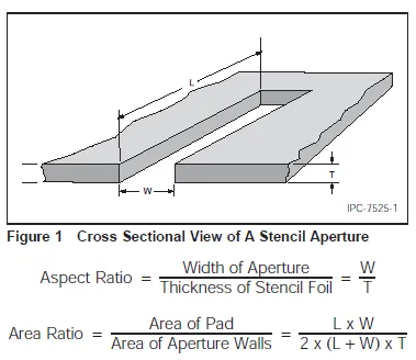
1. Aperture Design and Area Ratio
The size and shape of the stencil apertures must match the pad design and component requirements. The area ratio—calculated as the aperture’s open area divided by the wall area—should ideally be above 0.66 for good paste release. If the area ratio is too low, solder paste may stick to the aperture walls, leading to inconsistent deposits regardless of stencil thickness.
2. Solder Paste Type and Particle Size
The type of solder paste and its particle size should align with the stencil thickness and aperture size. For thinner stencils (e.g., 0.10 mm) used with fine-pitch components, smaller particle sizes (Type 4 or 5) ensure smooth printing and prevent clogging. Using the wrong paste type can negate the benefits of a well-chosen stencil thickness.
3. Printing Pressure and Speed
The pressure and speed of the squeegee during printing affect how evenly solder paste fills the apertures. Excessive pressure can cause paste to smear, while insufficient pressure may leave gaps. Adjusting these parameters ensures that the solder paste volume dictated by the stencil thickness is applied consistently.
4. Stepped Stencils for Mixed Assemblies
In boards with both fine-pitch and larger components, a single stencil thickness may not suit all areas. Stepped stencils, which have varying thicknesses in different regions, can address this issue. For example, a stencil might be 0.10 mm thick in areas with fine-pitch components and 0.15 mm thick near larger connectors, optimizing solder paste volume across the board.
Choosing the Right Stencil Thickness for Your Project
Selecting the appropriate stencil thickness is a balancing act that depends on your specific PCB design and component mix. Here are some general guidelines to help you make the right choice:
- For Fine-Pitch Components (e.g., 0201, BGAs): Use thinner stencils (0.08-0.10 mm) to limit solder paste volume and prevent bridging.
- For Standard Components (e.g., 0402, 0603): A stencil thickness of 0.12 mm is often ideal for achieving a good balance of solder volume.
- For Larger Components (e.g., connectors, through-hole): Opt for thicker stencils (0.15 mm or more) to ensure sufficient solder for strong mechanical bonding.
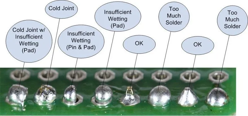
It’s also wise to conduct test runs with different stencil thicknesses during the prototyping phase. Inspect the solder joints post-reflow using X-ray or visual inspection to identify issues like bridging or insufficient solder. Adjust the thickness and other stencil printing parameters as needed to optimize PCB assembly quality.
Common Challenges and Solutions in Stencil Printing
Even with the right stencil thickness, challenges can arise during the printing process. Here are some common issues and how to address them for better solder joint quality:
1. Solder Paste Smearing
Smearing occurs when paste spreads beyond the pad due to excessive pressure or a misaligned stencil. Solution: Reduce squeegee pressure and ensure proper stencil alignment with the PCB.
2. Incomplete Paste Transfer
If paste doesn’t fully transfer through the apertures, it may be due to a low area ratio or clogged apertures. Solution: Clean the stencil regularly and check if the area ratio meets the recommended threshold of 0.66.
3. Inconsistent Solder Joints Across the Board
Variations in solder joint quality can result from uneven printing or PCB warpage. Solution: Use a stable fixture to hold the PCB flat during printing and verify that the stencil thickness suits all component types on the board.
Future Trends in Stencil Design and PCB Assembly Quality
As electronics continue to shrink and component densities increase, stencil design and printing techniques are evolving. Innovations like nano-coated stencils improve paste release for ultra-fine apertures, while advanced inspection systems help detect printing defects in real-time. Staying updated on these trends can give PCB manufacturers an edge in achieving superior solder joint quality.
Moreover, the growing adoption of mixed assemblies—combining fine-pitch surface-mount components with larger through-hole parts—will likely increase the use of stepped stencils. These designs allow for tailored solder paste volumes across different board areas, ensuring optimal results regardless of component diversity.
Conclusion: Mastering Stencil Thickness for Superior Solder Joints
Stencil thickness is a critical factor in determining solder joint quality during PCB assembly. By controlling the solder paste volume, it directly affects the electrical and mechanical integrity of the joints. Choosing the right thickness—along with optimizing other stencil printing parameters like aperture design, paste type, and printing settings—can significantly enhance PCB assembly quality.
Whether you’re dealing with fine-pitch components or larger connectors, understanding the impact of stencil thickness empowers you to make informed decisions and avoid common soldering defects. Take the time to test and refine your process, and you’ll see the difference in the reliability and performance of your electronic products.


