 ALLPCB


In the world of electronics manufacturing, controlling costs without sacrificing quality is a top priority. One key strategy that significantly impacts PCB assembly cost is panelization. But how exactly does panelization affect costs, and what savings can it bring? In short, panelization reduces PCB assembly costs by optimizing material utilization, improving manufacturing efficiency, and minimizing waste—often saving up to 20-30% on production expenses for large runs. This blog post dives deep into the role of panelization in cost reduction strategies, exploring its benefits, challenges, and best practices for maximizing savings.
What is PCB Panelization and Why Does It Matter?
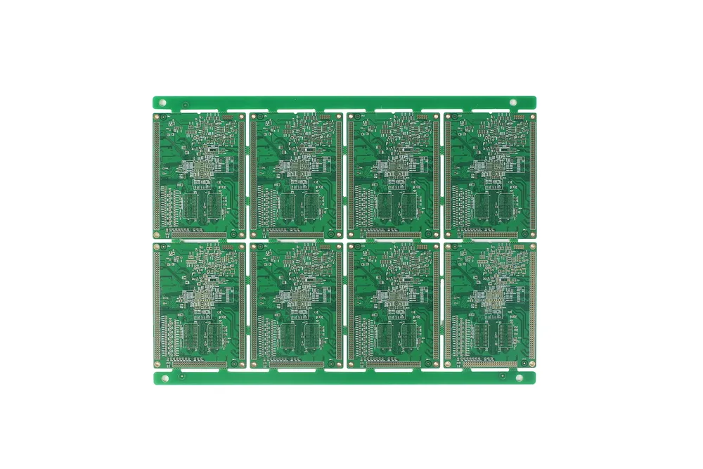
PCB panelization is the process of grouping multiple individual printed circuit boards (PCBs) into a single larger panel for manufacturing. Instead of producing each PCB separately, manufacturers create a panel that holds several boards, which are later separated after assembly. This technique is widely used in high-volume production to streamline processes and cut costs.
Panelization matters because it directly influences manufacturing efficiency and material utilization. By processing multiple boards at once, manufacturers can reduce setup times, lower handling costs, and make better use of raw materials. For businesses looking to optimize PCB assembly cost, panelization is a game-changer, especially when balancing quality and budget constraints.
How Panelization Reduces PCB Assembly Cost
Panelization offers several cost-saving benefits that impact the overall PCB assembly cost. Let’s break down the key ways it contributes to savings:
1. Improved Material Utilization
One of the biggest advantages of panelization is better material utilization. When individual PCBs are manufactured separately, there’s often wasted material around the edges of each board. Panelization arranges multiple boards on a single sheet, minimizing unused space. For instance, a panel measuring 18x24 inches might hold 10-20 small PCBs, reducing material waste by up to 15% compared to individual fabrication.
This efficient use of materials directly lowers the cost per board, especially for smaller designs where raw material expenses can add up quickly. By maximizing the number of boards per panel, manufacturers spend less on substrates like FR-4, a common PCB material, leading to significant cost reduction over large production runs.
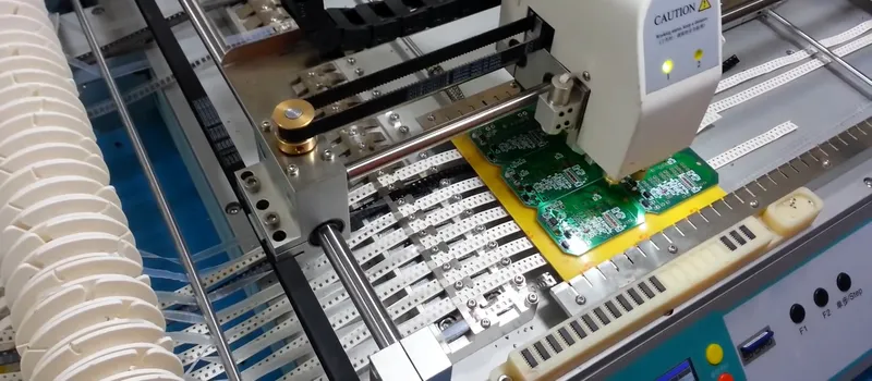
2. Faster Manufacturing Efficiency
Panelization streamlines the manufacturing process by allowing multiple boards to be processed simultaneously. During assembly, pick-and-place machines can populate components on several PCBs in one go, reducing machine setup time and labor costs. For example, assembling a panel of 12 boards might take only slightly longer than assembling a single board, cutting per-unit assembly time by as much as 50% in high-volume scenarios.
This boost in manufacturing efficiency translates to lower PCB assembly costs. Reduced machine runtime and fewer manual interventions mean manufacturers can handle larger orders faster, passing those savings on to customers.
3. Lower Handling and Testing Costs
Handling individual PCBs during assembly, testing, and shipping is time-consuming and costly. Panelization reduces the number of separate units that need to be moved, tested, and packaged. For instance, testing a single panel with 10 boards is far quicker than testing 10 individual boards, often saving 10-20% on quality control expenses.
Additionally, panelized boards are less prone to damage during handling since they’re processed as a single unit until the final stages. This reduces the risk of costly defects, further contributing to panelization cost savings.
Challenges of Panelization in Cost Management
While panelization offers clear cost-saving benefits, it’s not without challenges. Understanding these hurdles is crucial for implementing effective cost reduction strategies.
1. Increased Upfront Design Costs
Designing a panelized layout requires careful planning to ensure boards fit efficiently without compromising functionality. Engineers must account for spacing, breakaway tabs, or V-cuts for separation, and fiducial markers for alignment during assembly. This design work can add 5-10% to initial project costs, especially for complex or custom PCB shapes.
However, these upfront costs are often offset by savings in high-volume production. For smaller runs, the added design expense might outweigh the benefits, so it’s essential to evaluate production volume before opting for panelization.
2. Material Waste in Poorly Optimized Panels
If a panel layout isn’t optimized, material utilization can suffer, negating cost savings. For example, irregular PCB shapes or excessive spacing between boards can lead to wasted material, increasing costs by up to 10% per panel. To avoid this, designers must use software tools to maximize board density while adhering to manufacturing constraints like minimum edge clearances (typically 0.1-0.2 inches).
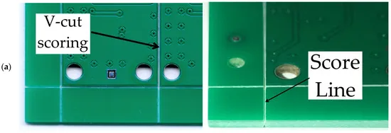
3. Depanelization Costs and Risks
After assembly, panelized boards must be separated through a process called depanelization, which can introduce additional costs and risks. Methods like V-scoring or tab routing require specialized equipment, adding 2-5% to production costs. If not done carefully, depanelization can also damage boards, leading to yield losses of 1-3% in some cases.
To minimize these risks, manufacturers often use precise cutting tools and test separation methods during prototyping to ensure clean breaks without stressing components.
Cost Reduction Strategies Through Effective Panelization
To fully leverage panelization for PCB assembly cost savings, consider the following strategies. These practical tips can help optimize material utilization and manufacturing efficiency while avoiding common pitfalls.
1. Optimize Panel Layout for Maximum Board Density
Work closely with your manufacturing team to design a panel layout that fits as many PCBs as possible without violating design rules. For example, a standard panel size of 18x24 inches might accommodate 15 boards with a 0.1-inch spacing between them. Using software to simulate layouts can help achieve up to 90% material utilization, directly lowering costs.
2. Standardize Board Sizes and Shapes
Whenever possible, design PCBs with uniform dimensions or shapes that tessellate well on a panel. Square or rectangular boards are easier to arrange without wasting space compared to irregular shapes. Standardization can reduce material costs by 5-10% and simplify the panelization process, enhancing manufacturing efficiency.
3. Balance Panel Size with Production Volume
Choosing the right panel size is critical for cost savings. Larger panels are more cost-effective for high-volume runs due to better material utilization, but they can be wasteful for small batches. For low-volume orders, smaller panels or shared panels (where multiple designs share the same panel) can reduce costs by 10-15% compared to full-size panels.
4. Use Cost-Effective Depanelization Methods
Select a depanelization method that balances cost and precision. V-scoring, which involves cutting shallow grooves for easy separation, is often the cheapest option, costing around $0.05-$0.10 per board. Tab routing, while more precise for complex shapes, can cost $0.20-$0.30 per board due to additional tooling. Evaluate the trade-offs based on your design needs to keep expenses low.
Real-World Impact: Panelization Cost Savings in Action
To illustrate the impact of panelization on PCB assembly cost, consider a hypothetical production run of 1,000 small PCBs, each measuring 2x2 inches. Without panelization, manufacturing these boards individually might cost $5 per board, totaling $5,000. This includes material waste, individual handling, and repeated machine setups.
With panelization, the same 1,000 boards could be arranged on 50 panels, each holding 20 boards. The cost per panel might be $60, totaling $3,000 for the run. This represents a 40% reduction in cost, driven by better material utilization (reducing waste by 10-15%) and improved manufacturing efficiency (cutting assembly time by 50%). Even after factoring in depanelization costs of $0.10 per board ($100 total), the savings remain substantial at $1,900.
This example highlights how panelization cost savings scale with volume, making it an essential strategy for large production runs. For smaller batches, the savings might be less pronounced but still significant when layouts are optimized.
Factors Influencing Panelization Cost Savings
Not all projects benefit equally from panelization. Several factors influence the level of cost savings achieved:
- Production Volume: High-volume runs (1,000+ units) typically see 20-30% cost reductions due to economies of scale, while low-volume runs (under 100 units) might save only 5-10%.
- Board Size and Shape: Smaller, regular-shaped boards panelize more efficiently, maximizing material utilization and savings.
- Complexity of Assembly: Boards with dense component layouts may require more precise panelization and depanelization, slightly increasing costs by 2-5%.
- Material Type: High-cost materials like flexible or high-frequency substrates amplify the savings from panelization, as waste reduction has a bigger financial impact.
Understanding these factors helps in tailoring panelization strategies to specific projects, ensuring maximum cost reduction without compromising quality.
Conclusion: Maximizing Savings with Strategic Panelization
Panelization is a powerful tool for reducing PCB assembly cost, offering savings through improved material utilization, enhanced manufacturing efficiency, and lower handling expenses. While challenges like upfront design costs and depanelization risks exist, they can be mitigated with careful planning and optimization. By adopting cost reduction strategies such as optimized layouts, standardized designs, and appropriate panel sizes, businesses can achieve significant savings—often 20-30% or more on large runs.
For engineers and manufacturers, the key takeaway is clear: panelization isn’t just a manufacturing technique; it’s a strategic approach to balancing cost and quality. By understanding its impact and applying best practices, you can drive down expenses while maintaining the high standards required in electronics production. Whether you’re managing a small prototype run or a large-scale project, panelization offers a path to smarter, more cost-effective PCB assembly.


