 ALLPCB


If you're looking to understand Surface Mount Technology (SMT) for Printed Circuit Board Assembly (PCBA), you've come to the right place. SMT is a method used to mount electronic components directly onto the surface of a PCB, making devices smaller, lighter, and more efficient. In this comprehensive guide, we'll dive deep into SMT PCBA assembly, explore SMT components, break down the SMT process, provide SMT design guidelines, and explain SMT reflow soldering. Whether you're an engineer, designer, or hobbyist, this blog will equip you with the knowledge to navigate SMT effectively.
What is Surface Mount Technology (SMT) in PCBA?
SMT, or Surface Mount Technology, is a manufacturing process where electronic components are placed and soldered directly onto the surface of a printed circuit board (PCB). Unlike older through-hole technology, where components have leads inserted into drilled holes, SMT allows for more compact designs and faster assembly. This technology is the backbone of modern electronics, enabling the production of everything from smartphones to industrial equipment.
In the context of PCBA, SMT plays a crucial role by streamlining the assembly process and reducing the size of the final product. With SMT, components are smaller, and boards can have components on both sides, maximizing space efficiency. This guide will walk you through every aspect of SMT for PCBA, ensuring you have a clear understanding of its benefits and implementation.
Understanding SMT Components
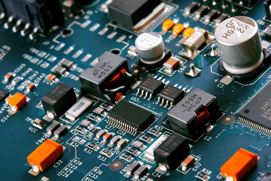
SMT components are specifically designed for surface mounting and are typically much smaller than their through-hole counterparts. These components come in various shapes and sizes, each suited for different functions on a PCB. Common SMT components include:
- Resistors and Capacitors: Often in tiny rectangular packages, measured in sizes like 0402 (0.04 x 0.02 inches) or 0603 (0.06 x 0.03 inches).
- Integrated Circuits (ICs): Available in packages like QFN (Quad Flat No-leads) or BGA (Ball Grid Array), which have pads or balls on the underside for soldering.
- Diodes and Transistors: Compact packages like SOT (Small Outline Transistor) for minimal footprint.
- Connectors: Designed for surface mounting to save space compared to bulky through-hole connectors.
The small size of SMT components allows for higher circuit density, meaning more functionality can fit into a smaller area. However, their miniature nature requires precise placement and soldering techniques, which we’ll cover later in the SMT process section.
The SMT PCBA Assembly Process: Step by Step
The SMT PCBA assembly process is a series of carefully orchestrated steps that ensure components are accurately placed and securely soldered onto the PCB. Below, we outline the key stages of this process, providing clarity on how modern electronics are brought to life.
1. Solder Paste Application
The process begins with applying solder paste to the PCB. Solder paste, a mixture of tiny solder particles and flux, is applied using a stencil that matches the PCB’s layout. This ensures paste is only placed on the pads where components will be mounted. Precision is critical here, as uneven paste can lead to poor connections.
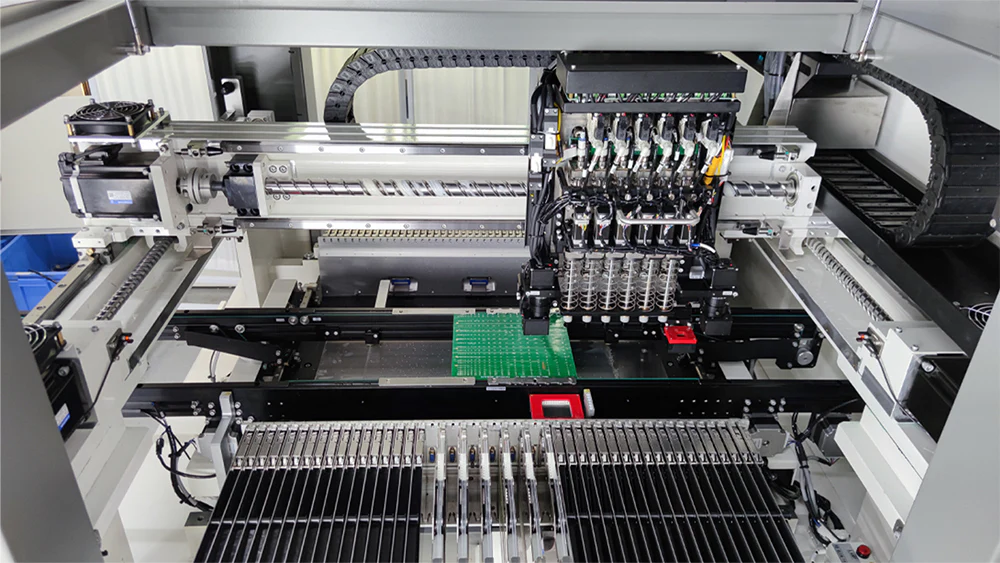
2. Component Placement
Next, automated machines, often called pick-and-place machines, position SMT components onto the solder paste. These machines can place thousands of components per hour with accuracy down to 0.01 mm, ensuring even the smallest parts are aligned correctly.
3. Reflow Soldering
Once components are placed, the PCB passes through a reflow oven. The oven heats the board in stages, melting the solder paste to form strong electrical connections between components and pads. This step, known as SMT reflow soldering, is vital for reliability and will be explored in detail later.
4. Inspection and Testing
After soldering, the board undergoes inspection using tools like Automated Optical Inspection (AOI) to detect defects such as misaligned components or solder bridges. Electrical testing ensures the board functions as intended, often checking for signal integrity at speeds up to 1 GHz for high-speed designs.
SMT Design Guidelines for Optimal Results
Designing a PCB for SMT assembly requires careful planning to avoid issues during manufacturing. Following SMT design guidelines can improve yield rates, reduce costs, and ensure reliability. Here are some key considerations for engineers and designers:
Component Placement
Place components with similar orientations to simplify assembly. For example, align all polarized components like capacitors in the same direction to minimize placement errors. Also, maintain a minimum spacing of 0.2 mm between components to prevent solder bridging.
Pad Design
Ensure pad sizes match the component specifications. For a 0402 resistor, pads should typically be 0.5 mm x 0.3 mm with a 0.4 mm gap between them. Oversized or undersized pads can lead to weak solder joints or tombstoning (where one end of a component lifts off the pad).
Thermal Management
Consider heat dissipation in your design, especially for power components. Use thermal vias with a diameter of 0.3 mm and a pitch of 1.2 mm under high-power ICs to transfer heat to the opposite side of the board.
Solder Mask and Silkscreen
Apply a solder mask to prevent unintended solder flow, ensuring a clearance of 0.1 mm around pads. Keep silkscreen markings clear and outside component areas to avoid interference during assembly.
By adhering to these SMT design guidelines, you can create boards that are easier to manufacture and more reliable in operation. Always consult industry standards like IPC-7351 for detailed footprint recommendations.
SMT Reflow Soldering: The Heart of the Process
SMT reflow soldering is a critical step in the assembly process, where solder paste is melted to form permanent connections between components and the PCB. Understanding this process is essential for achieving high-quality results. Let’s break it down into its key phases and best practices.
Phases of Reflow Soldering
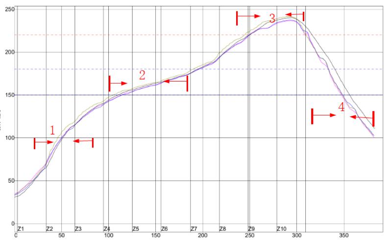
Reflow soldering happens in a controlled oven with a specific temperature profile, typically divided into four zones:
- Preheat Zone: The PCB is gradually heated to 150–180°C over 60–90 seconds to activate the flux in the solder paste and prevent thermal shock.
- Soak Zone: The temperature stabilizes at 180–200°C for 60–120 seconds, ensuring even heat distribution across the board.
- Reflow Zone: The temperature peaks at 220–250°C for 20–40 seconds, melting the solder to form joints. For lead-free solder, the peak is often closer to 245°C.
- Cooling Zone: The board cools down at a controlled rate of 2–4°C per second to solidify the solder without causing stress or cracks.
Best Practices for Reflow Soldering
To ensure successful SMT reflow soldering, follow these tips:
- Use the correct temperature profile based on your solder paste type (lead-free or leaded). Lead-free solder often requires a peak temperature 20–30°C higher than leaded solder.
- Monitor the conveyor speed in the reflow oven to maintain consistent heating. A speed of 0.8–1.2 meters per minute is typical for most ovens.
- Ensure proper ventilation to remove flux vapors, which can otherwise cause contamination or voids in solder joints.
Mastering SMT reflow soldering can significantly reduce defects like cold joints or component shifting, leading to more reliable PCBA outcomes.
Advantages of SMT in PCBA
SMT offers numerous benefits that make it the preferred choice for modern electronics manufacturing. Understanding these advantages can help you appreciate why SMT dominates the industry.
- Smaller Size: SMT components take up less space, allowing for compact designs critical in devices like wearables and IoT gadgets.
- Higher Speed: Automated SMT assembly lines can produce thousands of boards per day, far outpacing manual through-hole methods.
- Cost Efficiency: Reduced material usage and faster production lower overall costs, especially for high-volume runs.
- Improved Performance: Shorter signal paths in SMT designs reduce impedance, supporting high-frequency applications up to 5 GHz in some cases.
These benefits make SMT an ideal solution for creating cutting-edge electronics that meet today’s demands for size, speed, and efficiency.
Common Challenges in SMT PCBA Assembly and How to Overcome Them
While SMT offers many advantages, it also comes with challenges that can impact quality if not addressed. Here are some common issues and solutions:
Tombstoning
This occurs when a small component stands upright on one end due to uneven heating or pad design. To prevent it, ensure symmetrical pad sizes and balanced thermal profiles during reflow soldering.
Solder Bridging
Excess solder can connect adjacent pads, causing shorts. Use precise stencil designs and maintain a solder mask clearance of at least 0.1 mm to avoid this issue.
Component Misalignment
Misaligned components can result from incorrect pick-and-place settings. Regularly calibrate machines and use fiducial markers on the PCB for alignment accuracy within 0.05 mm.
By proactively addressing these challenges, you can achieve higher success rates in SMT PCBA assembly.
Conclusion: Mastering SMT for PCBA Success
Surface Mount Technology (SMT) is a game-changer for PCBA, enabling the creation of compact, high-performance electronics with unmatched efficiency. From understanding SMT components to mastering the SMT process, adhering to SMT design guidelines, and perfecting SMT reflow soldering, this guide has covered the essentials you need to succeed. By applying these insights, you can optimize your designs and manufacturing processes for better reliability and cost-effectiveness.
At ALLPCB, we’re committed to supporting your journey with SMT PCBA assembly. Whether you’re prototyping a new design or scaling up production, leveraging SMT effectively can make all the difference. Keep these principles in mind, and you’ll be well on your way to creating cutting-edge electronics that stand out in the market.


