 ALLPCB


Are you a PCB manufacturer looking to ensure the quality of your solder joints? Choosing the right solder joint inspection equipment is crucial for maintaining high standards in your production process. In this comprehensive buyer’s guide, we’ll explore the best solder joint inspection tools, including Automated Optical Inspection (AOI) systems and X-ray inspection equipment, while breaking down costs and key considerations for PCB inspection equipment price. Let’s dive into everything you need to know to make an informed decision for your manufacturing needs.
Why Solder Joint Inspection Matters for PCB Manufacturers
In the world of printed circuit board (PCB) manufacturing, solder joints are the backbone of reliable electronic assemblies. These tiny connections between components and the board must be flawless to ensure functionality and durability. A single defective solder joint can lead to failures, costly rework, or even product recalls. That’s where solder joint inspection equipment comes in. By detecting issues like insufficient solder, bridging, or voids early in the process, you can save time, reduce waste, and maintain customer trust.
Modern inspection tools use advanced technologies to identify defects that are invisible to the naked eye. Whether you’re dealing with surface-mount devices (SMDs) or complex ball grid arrays (BGAs), having the right equipment is essential for quality control. This guide will help you understand the options available and choose the best tools for your specific needs.
Types of Solder Joint Inspection Equipment
There are several types of equipment designed for inspecting solder joints, each with unique strengths. Below, we’ll cover the most common options to help you decide which fits your production line.
1. Automated Optical Inspection (AOI) Systems
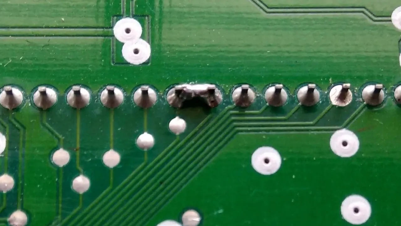
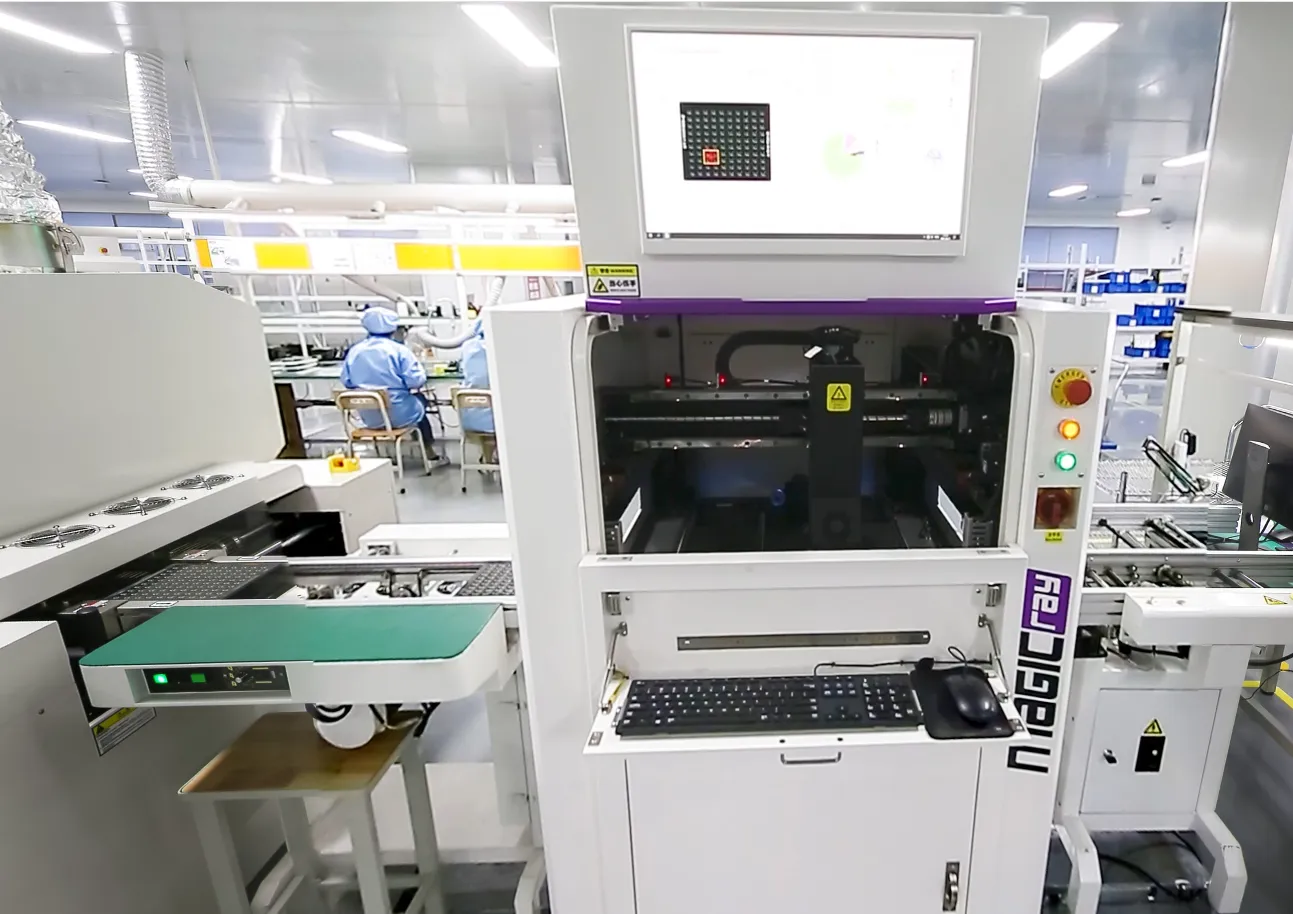
Automated Optical Inspection (AOI) systems are among the most widely used tools for solder joint inspection. These systems use high-resolution cameras and advanced lighting to capture detailed images of the PCB surface. Sophisticated software then analyzes these images to detect defects such as misaligned components, insufficient solder, or solder bridges.
AOI systems are ideal for high-volume production because they offer fast, non-contact inspection. They can process hundreds of boards per hour, with some systems achieving inspection speeds of up to 100 cm2 per second. However, AOI is limited to visible defects on the surface and cannot inspect hidden solder joints, such as those under BGAs.
Key Benefits of AOI Systems:
- High-speed inspection for large-scale production
- Non-destructive and non-contact method
- Accurate detection of surface-level defects
2. X-Ray Inspection Equipment
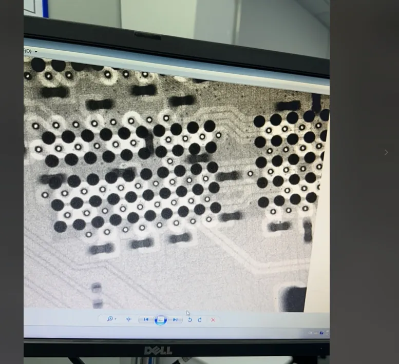
For hidden or complex solder joints, X-ray inspection equipment is the go-to solution. This technology uses X-rays to penetrate the PCB and create detailed images of internal structures. It’s particularly effective for inspecting BGAs, quad-flat no-leads (QFNs), and other components where solder joints are not visible from the surface.
X-ray systems can detect issues like voids in solder joints, which can compromise thermal and electrical conductivity. They are slower than AOI systems, often taking several seconds per component, but their ability to reveal hidden defects makes them indispensable for high-reliability applications like aerospace or medical devices.
Key Benefits of X-Ray Inspection:
- Non-destructive testing of hidden solder joints
- High accuracy for detecting internal defects like voids
- Essential for complex, multi-layer boards
3. Solder Paste Inspection (SPI) Systems
Solder Paste Inspection (SPI) systems focus on the quality of solder paste application before components are placed and reflowed. Using 3D imaging technology, SPI equipment measures the volume, height, and alignment of solder paste deposits. This early-stage inspection helps prevent defects before they occur, reducing rework costs.
SPI systems are often integrated into the production line alongside AOI systems. They can inspect paste deposits with precision, detecting variations as small as 10 micrometers. While they don’t directly inspect solder joints, they play a critical role in ensuring joint quality by catching issues at the source.
Key Benefits of SPI Systems:
- Prevents defects by inspecting solder paste application
- Highly precise 3D measurement capabilities
- Reduces rework by addressing issues early
Factors to Consider When Buying Solder Joint Inspection Equipment
Choosing the right equipment for your PCB manufacturing process involves evaluating several factors. Here’s a detailed breakdown to guide your decision-making process in this AOI system buyer guide and beyond.
1. Production Volume and Speed
Your production volume directly impacts the type of equipment you need. For high-volume manufacturing, an AOI system with a fast throughput—capable of inspecting up to 500 components per minute—is often the best choice for surface defects. However, if you produce smaller batches of complex boards, investing in X-ray inspection equipment might be more practical despite its slower speed.
2. Types of Defects and Components
Consider the types of components you work with and the defects you need to detect. If your boards primarily use SMDs with visible solder joints, an AOI system might suffice. For boards with BGAs or multi-layer designs, X-ray inspection equipment is non-negotiable to ensure hidden joints are defect-free.
3. Budget and Cost Considerations
The cost of PCB inspection equipment varies widely based on features, brand, and capabilities. Below, we’ll explore the general price ranges for different types of equipment to give you a clearer picture of X-ray inspection equipment cost and overall PCB inspection equipment price.
- AOI Systems: Entry-level AOI systems start at around $30,000, while high-end models with advanced software and faster processing can cost upwards of $150,000.
- X-Ray Inspection Equipment: Basic X-ray systems for small-scale use can start at $50,000, but industrial-grade equipment with automated features often ranges from $100,000 to $300,000.
- SPI Systems: Solder paste inspection tools typically cost between $40,000 and $120,000, depending on the level of precision and integration capabilities.
Keep in mind that these are approximate figures, and costs can vary based on customization, software upgrades, and maintenance packages. Factor in long-term costs like training, calibration, and repairs when budgeting.
4. Ease of Use and Integration
Modern inspection equipment often comes with user-friendly interfaces, but some systems require extensive training to operate effectively. Look for tools with intuitive software and compatibility with your existing production line. Integration with other systems, such as automated defect reporting or data analytics, can streamline your workflow and improve efficiency.
5. Maintenance and Support
Regular maintenance is essential to keep inspection equipment running smoothly. Check if the supplier offers local support, spare parts availability, and software updates. Downtime due to equipment failure can be costly, so prioritize vendors with a strong reputation for after-sales service.
Best Solder Joint Inspection Tools: Features to Look For
When shopping for the best solder joint inspection tools, focus on features that align with your manufacturing goals. Here are some must-have capabilities to consider:
- High-Resolution Imaging: For AOI and SPI systems, look for cameras with at least 5-megapixel resolution to capture fine details. For X-ray systems, ensure the equipment offers clear 2D or 3D imaging for accurate defect detection.
- Automated Defect Classification: Advanced software can automatically classify defects, reducing manual review time. Some systems achieve up to 95% accuracy in defect identification.
- Flexibility: Choose equipment that can handle a range of board sizes and component types. Adjustable settings for different PCB thicknesses (e.g., 0.5 mm to 5 mm) are a plus.
- Data Analytics: Tools with built-in analytics can track defect trends over time, helping you identify recurring issues in your process.
Balancing Cost and Quality in PCB Inspection Equipment Price
Finding the right balance between cost and quality is a common challenge for PCB manufacturers. While it’s tempting to opt for the cheapest option, low-cost equipment may lack the precision or durability needed for consistent results. On the other hand, overspending on high-end systems might not be necessary if your production needs are straightforward.
Start by defining your minimum requirements. For example, if you only need to inspect visible solder joints on simple boards, a mid-range AOI system priced around $50,000 to $80,000 could be sufficient. If your products demand the highest reliability, such as in automotive or medical applications, investing in a premium X-ray system with advanced imaging might be worth the $200,000 price tag.
Don’t forget to explore financing options or leasing programs, which can spread out the cost over time. Some suppliers also offer modular systems that allow you to upgrade features as your budget allows.
How to Choose the Right Vendor for Solder Joint Inspection Equipment
Selecting a reliable vendor is just as important as choosing the equipment itself. A good supplier will provide not only high-quality tools but also ongoing support to ensure your investment pays off. Here are some tips for finding the right partner:
- Industry Experience: Work with vendors who have a proven track record in the PCB manufacturing sector. They’re more likely to understand your specific challenges and needs.
- Demo Opportunities: Request a live demonstration or trial period to test the equipment in your production environment before committing.
- Customer Reviews: Look for feedback from other manufacturers about the vendor’s products and services. Online forums and industry groups can be valuable resources.
- Training and Support: Ensure the vendor offers comprehensive training for your team and has a responsive technical support team to address issues quickly.
Future Trends in Solder Joint Inspection Technology
The field of solder joint inspection is evolving rapidly, driven by advancements in automation and artificial intelligence (AI). Here are some trends to watch that could shape your future equipment purchases:
- AI-Powered Defect Detection: AI algorithms are improving defect recognition rates, with some systems achieving false call rates below 0.1%. This reduces the need for manual verification.
- Integration with Industry 4.0: Inspection equipment is increasingly connected to smart factory systems, enabling real-time data sharing and predictive maintenance.
- Portable Inspection Tools: Compact, portable X-ray and AOI systems are emerging, offering flexibility for smaller manufacturers or on-site inspections.
Conclusion: Making an Informed Decision for Your PCB Manufacturing Needs
Investing in solder joint inspection equipment is a critical step for PCB manufacturers aiming to deliver high-quality, reliable products. Whether you opt for an AOI system for fast surface inspections, X-ray equipment for hidden defects, or an SPI system for early-stage quality control, understanding your production needs and budget is key. By focusing on the best solder joint inspection tools with features like high-resolution imaging and automated defect classification, you can enhance your quality assurance process.
Take the time to evaluate different options, consider the long-term costs of PCB inspection equipment price, and partner with a trusted vendor. With the right tools in place, you’ll be well-equipped to meet the demands of modern electronics manufacturing and ensure the integrity of every solder joint on your boards.
At ALLPCB, we’re committed to supporting PCB manufacturers with resources and insights to optimize their processes. Stay tuned for more guides and updates on the latest in PCB technology and equipment.


