ALLPCB


In the fast-paced world of electronics, getting a product to market quickly can make or break its success. Prototype assembly is a critical step in this journey, allowing engineers to test and refine designs before committing to full-scale production. A well-executed prototype phase can catch design flaws early, reduce costly revisions, and accelerate your time-to-market. In this blog, we share actionable tips to streamline your printed circuit board (PCB) prototype assembly process, helping you deliver high-quality products faster.
Whether you're designing a consumer gadget or an industrial IoT device, these strategies will help you optimize your prototyping workflow, minimize delays, and ensure your PCBs meet performance expectations. Let's dive into the key steps to achieve a faster, more efficient prototype assembly process.
Why Prototype Assembly Matters for Time-to-Market
Prototyping is more than a preliminary step—it's the foundation of a successful product launch. By creating and testing a functional PCB prototype, engineers can validate designs, identify issues, and refine performance before mass production. According to industry data, catching a design flaw during prototyping can reduce development costs by up to 10x compared to fixing it after production begins. A streamlined prototype assembly process not only saves time and money but also gives you a competitive edge in today's rapid innovation cycles.
1. Start with a Robust Design for Manufacturability (DFM)
A common roadblock in prototype assembly is a design that's difficult or costly to manufacture. Designing for Manufacturability (DFM) ensures your PCB is optimized for assembly, reducing errors and speeding up production. Here's how to incorporate DFM principles:
- Simplify Component Placement: Place components logically to minimize trace lengths and avoid complex routing. For example, keep high-speed signal components close to their connectors to reduce signal integrity issues, such as crosstalk or impedance mismatches (target impedance: ~50 ohms for single-ended signals).
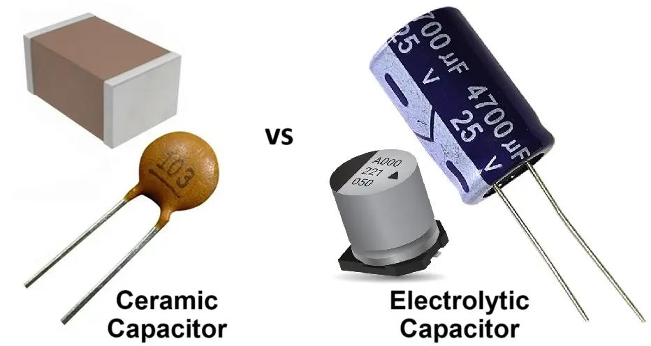
- Standardize Components: Use standard, readily available components to avoid supply chain delays. For instance, opting for a common 0805 resistor size instead of a niche 0201 can cut lead times significantly.
- Minimize Layer Count: Unless your design requires high-density interconnects (HDI), aim for fewer layers (e.g., 2-4 layers) to reduce fabrication time and costs. A 4-layer board typically takes 1-2 days less to prototype than an 8-layer board.
By prioritizing DFM, you can avoid costly redesigns and ensure your prototype is ready for assembly with minimal hiccups.

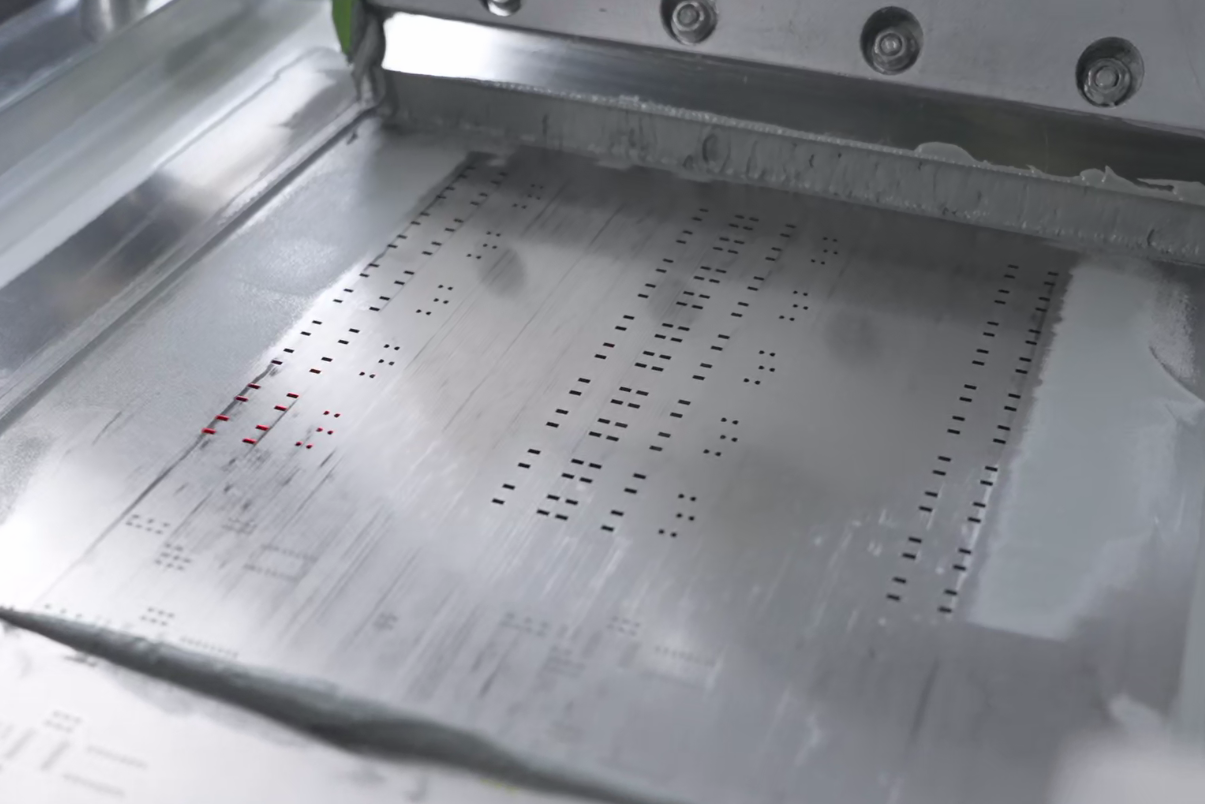
2. Leverage Rapid Prototyping Services
Time is of the essence in prototype assembly, and choosing a manufacturer with quick-turn capabilities can shave days or even weeks off your timeline. Rapid prototyping services prioritize speed without compromising quality, often delivering fully assembled PCBs in as little as 24-48 hours. Here's how to make the most of these services:
- Choose a Reliable Partner: Select a manufacturer with a proven track record in quick-turn prototyping. Look for capabilities like automated optical inspection (AOI) and X-ray testing to ensure quality.
- Submit Clean Design Files: Provide Gerber files, a bill of materials (BOM), and precise assembly instructions to avoid back-and-forth with the manufacturer. Incomplete files can delay production by 1-3 days.
- Opt for Turnkey Solutions: Turnkey services, where the manufacturer handles component sourcing, fabrication, and assembly, can reduce coordination time. For example, a turnkey provider can source a 100 nF capacitor in hours, compared to days if you're managing procurement yourself.
By partnering with a rapid prototyping service, you can iterate quickly and keep your project on track.
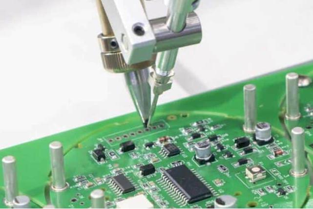
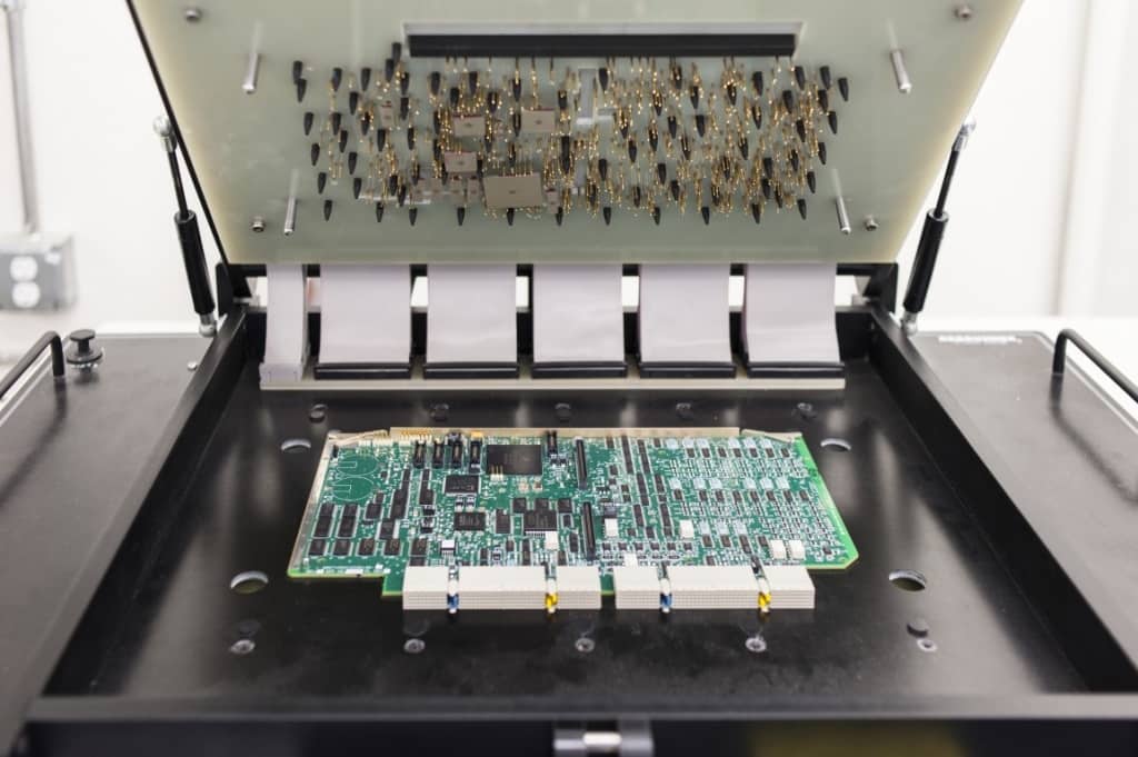
3. Prioritize Functional Testing Early
Functional testing during the prototype phase is critical to catching issues before they escalate. A functional circuit test (FCT) fixture, which simulates real-world operating conditions, can validate your PCB's performance under power. Here's how to integrate testing effectively:
- Test for Signal Integrity: For high-speed designs, verify signal integrity to avoid issues like reflections or crosstalk. For instance, a 3.5 GHz signal requires controlled impedance traces (typically 50-100 ohms) to maintain performance.
- Simulate Real-World Conditions: Test your prototype under varying temperatures (e.g., -40°C to 85°C for industrial applications) and power conditions to ensure reliability.
- Automate Where Possible: Use automated test equipment (ATE) to run repetitive tests, such as checking voltage levels at key nodes (e.g., 3.3V or 5V rails), to save time and improve accuracy.
Early testing reduces the risk of costly rework and ensures your design is production-ready.
4. Optimize Component Selection for Availability
Component shortages can derail your prototyping timeline. In 2024, global supply chain challenges delayed 30% of electronics projects by an average of 2-4 weeks. To avoid this, focus on component availability:
- Check Stock Early: Use distributor databases to confirm component availability before finalizing your design. For example, a microcontroller like the STM32F4 series may have shorter lead times than a niche FPGA.
- Specify Alternatives: Include alternate components in your BOM with compatible footprints and specs. For instance, if a 10 kΩ resistor is unavailable, list a substitute with the same 1% tolerance and 0805 package.
- Avoid Obsolete Parts: Cross-reference component lifecycle status to avoid parts nearing end-of-life, which can cause delays if replacements are needed.
Proactive component selection keeps your prototype assembly on schedule and minimizes supply chain risks.
5. Streamline Assembly with Clear Documentation
Clear documentation is the backbone of efficient prototype assembly. Ambiguities in your design files or instructions can lead to errors, adding days to your timeline. Follow these best practices:
- Detailed BOM: Include part numbers, quantities, and specific tolerances (e.g., ±5% for capacitors). A clear BOM reduces procurement errors by up to 80%.
- Assembly Drawings: Provide diagrams showing component placement, orientation, and special instructions (e.g., 'Mount C1 vertically to avoid thermal stress').
- Silkscreen Clarity: Ensure your PCB's silkscreen includes clear labels for component references and polarity markers to prevent assembly mistakes, such as a reversed diode causing a short circuit.
Comprehensive documentation enables your manufacturer to assemble prototypes quickly and accurately.

6. Iterate Quickly with Modular Designs
Modular PCB designs allow you to test specific sections of your circuit independently, speeding up debugging and iteration. For example, separating power management and signal processing into distinct modules can reduce troubleshooting time by 50%. Here's how to implement modularity:
- Use Breakout Boards: Design critical components, like a high-frequency RF module, on separate breakout boards for isolated testing.
- Incorporate Test Points: Add test points for key signals (e.g., clock lines at 100 MHz) to simplify debugging without disassembling the entire board.
- Standardize Interfaces: Use common connectors, like USB-C or pin headers, to swap modules quickly during testing.
Modular designs enable faster iterations, helping you refine your prototype without starting from scratch.
7. Address High-Frequency Design Challenges
For PCBs operating at high frequencies (e.g., >1 GHz), signal integrity and electromagnetic compatibility (EMC) are critical. Poor handling of these factors can lead to performance issues that delay market entry. Key considerations include:
- Controlled Impedance: Design traces with precise impedance (e.g., 50 ohms for RF signals) to minimize signal loss. A mismatch of just 10 ohms can degrade signal quality by 20%.
- Ground Planes: Use continuous ground planes to reduce electromagnetic interference (EMI). For example, a 4-layer board with a dedicated ground layer improves EMI performance by 15-20% compared to a 2-layer board.
- Via Optimization: Minimize via usage in high-frequency paths, as each via can introduce 0.5-1 nH of inductance, disrupting signal integrity.
Addressing these challenges during prototyping ensures your PCB performs reliably in real-world applications.
8. Collaborate with Your Manufacturer Early
Engaging your PCB manufacturer during the design phase can prevent costly delays. Manufacturers can provide insights into material availability, fabrication constraints, and assembly feasibility. For example:
- Material Selection: Consult on substrate materials like FR-4 (dielectric constant: ~4.5) for standard applications or Rogers 4350 (dielectric constant: ~3.5) for high-frequency designs.
- Feasibility Reviews: Request a design review to catch issues like trace widths below 4 mil, which may be unmanufacturable on standard equipment.
- Prototyping Feedback: Use manufacturer feedback to refine your design, such as adjusting solder mask clearances to prevent bridging during assembly.
Early collaboration aligns your design with manufacturing capabilities, reducing lead times.
How ALLPCB Supports Your Prototyping Goals
At ALLPCB, we understand the importance of speed and precision in prototype assembly. Our quick-turn prototyping services deliver fully assembled PCBs in as little as 24 hours, supported by global logistics to ensure timely delivery. With advanced manufacturing capabilities, including automated optical inspection and turnkey component sourcing, we help engineers validate designs efficiently. Whether you need a single-layer board or a complex multilayer design, our team is dedicated to accelerating your time-to-market while maintaining the highest quality standards.
Conclusion: Accelerate Your Path to Market
Efficient prototype assembly is the key to bringing your electronic products to market faster. By focusing on DFM, leveraging rapid prototyping services, prioritizing testing, and collaborating with your manufacturer, you can streamline the process and avoid costly delays. Implementing these tips—backed by clear documentation, modular designs, and high-frequency considerations—ensures your PCB prototypes are functional, reliable, and ready for production.
Start applying these strategies today to reduce your development timeline and gain a competitive edge. If you're ready to take your prototype to the next level, partner with a trusted manufacturer to bring your vision to life.