 ALLPCB


Are you struggling with hidden solder joint defects in Ball Grid Array (BGA) components that impact your PCB performance? X-Ray inspection is the key to uncovering issues like open circuits, shorts, voids, and head-in-pillow defects that are invisible to the naked eye. In this detailed guide, we’ll explore how X-Ray inspection for BGA solder joint defects works, the specific problems it can detect, and why it’s critical for ensuring reliability in high-density electronics. Whether you're an electrical engineer troubleshooting a failed board or optimizing a manufacturing process, this post will provide actionable insights to enhance your results.
Why BGA Solder Joint Defects Matter in Electronics
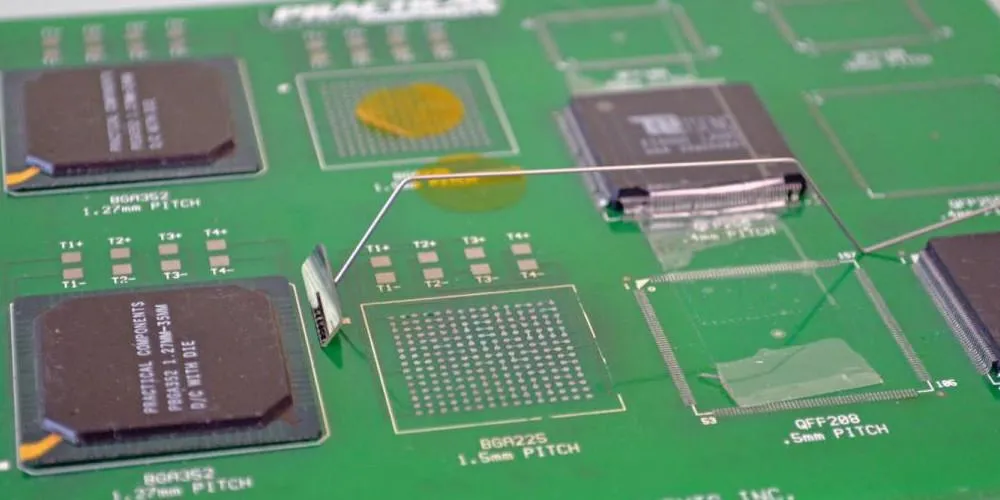
Ball Grid Array (BGA) components are widely used in modern electronics due to their ability to support high-density interconnections in a compact footprint. With hundreds or even thousands of solder balls (sometimes exceeding 208 leads) hidden beneath the package, BGAs are ideal for high I/O devices like microprocessors and GPUs. However, this design also makes them prone to hidden solder joint defects that can lead to performance issues or outright failure.
Common defects include open circuits, shorts, voids, and head-in-pillow (HIP) issues. These problems can cause intermittent connections, reduced thermal performance, or complete device failure. For electrical engineers, undetected defects during manufacturing or testing can result in costly rework, product recalls, or damaged reputations. This is where X-Ray inspection becomes indispensable—it’s the only reliable way to see beneath the BGA package and identify issues before they escalate.
What Are the Common BGA Solder Joint Defects?
Before diving into X-Ray inspection techniques, let’s break down the most common BGA solder joint defects that engineers encounter. Understanding these issues will help you appreciate why advanced inspection methods are necessary.
1. Open Circuits in BGA Solder Joints
An open circuit occurs when a solder ball fails to make proper contact with the PCB pad, often due to insufficient solder paste, misalignment during placement, or thermal stress during reflow. This defect can lead to a complete loss of electrical connection, disrupting signal flow. For instance, in a high-speed design operating at 5 GHz, an open circuit can cause signal integrity issues, resulting in data errors or system crashes.
2. Shorts in BGA Connections
Shorts happen when solder bridges form between adjacent balls, creating unintended electrical connections. This can result from excess solder paste or poor stencil design. Shorts are particularly problematic in power delivery networks, where they can cause overcurrent conditions, overheating, or even component burnout. Detecting BGA shorts with X-Ray is critical to avoid such catastrophic failures.
3. Voids in Solder Joints
Voids are air pockets or gaps within the solder joint, often caused by outgassing during the reflow process or poor wetting of the solder. Excessive voiding (e.g., voids occupying more than 25% of the joint area) can weaken the mechanical strength of the connection and impair thermal conductivity. In high-power applications, this can lead to overheating, with junction temperatures rising beyond safe limits like 125°C.
4. Head-in-Pillow (HIP) Defects
Head-in-pillow defects occur when the solder ball and solder paste fail to fully coalesce during reflow, creating a weak or non-existent bond that resembles a "head resting on a pillow." This defect is often linked to warpage of the BGA package or PCB under thermal stress. HIP defects are notorious for causing intermittent failures, making them challenging to diagnose without proper tools like X-Ray inspection for BGA head-in-pillow issues.
How X-Ray Inspection Reveals Hidden BGA Defects
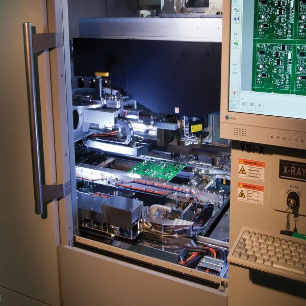
Unlike visual inspection or automated optical inspection (AOI), which can only assess surface-level features, X-Ray inspection penetrates through materials to reveal the internal structure of BGA solder joints. This non-destructive testing method uses X-rays to create detailed 2D or 3D images of the hidden connections, allowing engineers to spot defects that would otherwise go unnoticed.
The Basics of X-Ray Inspection for BGA Solder Joints
X-Ray systems work by passing high-energy rays through the PCB assembly. Dense materials like solder absorb more rays and appear darker in the resulting image, while less dense areas like voids or gaps appear lighter. Modern X-Ray machines can achieve resolutions down to 1 micron, making them capable of detecting even tiny anomalies in solder joints with diameters as small as 0.3 mm.
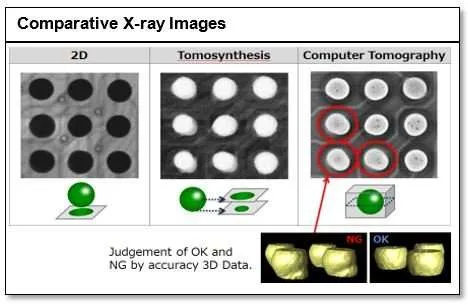
For BGA inspection, two primary techniques are used: 2D X-Ray imaging and 3D Computed Tomography (CT) X-Ray. Each has its strengths, depending on the complexity of the defect and the level of detail required.
2D X-Ray Imaging for Quick Defect Detection
2D X-Ray imaging provides a top-down or angled view of the BGA solder joints. It’s a fast and cost-effective method for detecting obvious issues like open circuits, shorts, and large voids. For example, a solder bridge between two balls will appear as an irregular dark mass connecting them, while an open circuit might show a gap or incomplete solder fill at the pad interface.
However, 2D X-Ray has limitations—it can’t always distinguish overlapping structures or provide depth information. This makes it less effective for complex defects like head-in-pillow, where the issue lies in the vertical alignment of the joint.
3D CT X-Ray for In-Depth Analysis
3D CT X-Ray takes inspection to the next level by reconstructing a three-dimensional model of the BGA assembly. By taking multiple 2D images from different angles and combining them, 3D CT can reveal the exact location and nature of defects in all dimensions. For instance, it can clearly show a head-in-pillow defect by displaying the separation between the solder ball and paste in a cross-sectional view.
While 3D CT is more time-consuming and expensive, it’s invaluable for high-reliability applications like aerospace or medical devices, where failure is not an option. Some systems can even quantify void percentages with precision, helping engineers assess whether a joint meets industry standards like IPC-A-610, which often specifies a maximum void area of 25% for critical applications.
Targeted X-Ray Inspection for Specific BGA Defects
Now that we’ve covered the general principles of X-Ray inspection, let’s dive into how it specifically addresses each type of BGA solder joint defect. This will help you understand which techniques to prioritize based on the issues you’re facing.
X-Ray Inspection for BGA Open Circuits
Open circuits are often visible in 2D X-Ray images as a lack of solder fill or a clear separation between the ball and pad. Engineers can use angled X-Ray views to confirm the disconnection, especially if the issue is subtle. For high-speed designs, detecting opens early is critical to avoid signal loss—imagine a 10 Gbps data line failing due to a single disconnected pin.
BGA Shorts Detection with X-Ray
Shorts appear as dark, irregular shapes connecting adjacent solder balls in X-Ray images. A high-resolution 2D X-Ray system can typically spot bridges down to 50 microns in width. By identifying shorts during inspection, engineers can adjust reflow profiles or stencil designs to prevent recurrence, saving boards from potential short-circuit damage during operation.
BGA Void Detection Using X-Ray
Voids show up as lighter spots within the darker solder joint in X-Ray images due to their lower density. Advanced software in modern X-Ray systems can calculate the void percentage automatically, helping engineers determine if the joint meets reliability standards. For thermal management, minimizing voids is crucial—excessive voiding can increase thermal resistance by 20% or more, pushing component temperatures beyond safe limits.
X-Ray Inspection of BGA Head-in-Pillow Defects
Head-in-pillow defects are trickier to detect and often require 3D CT X-Ray for accurate diagnosis. In a cross-sectional view, HIP appears as a distinct separation between the solder ball and paste, indicating poor bonding. This defect is a common cause of intermittent failures in devices subjected to thermal cycling, where temperature swings from -40°C to 85°C can exacerbate weak connections.
Benefits of X-Ray Inspection in BGA Manufacturing and Testing
Implementing X-Ray inspection in your BGA assembly process offers several advantages, especially for engineers working on high-reliability or high-performance electronics.
- Non-Destructive Testing: X-Ray inspection allows you to evaluate solder joints without damaging the board, preserving valuable prototypes or production units.
- Early Defect Detection: Identifying issues like voids or shorts during manufacturing prevents costly failures in the field, reducing warranty claims and rework expenses.
- Process Optimization: X-Ray data can reveal trends in defects, helping you fine-tune reflow profiles, solder paste volume, or component placement accuracy. For example, reducing peak reflow temperature by just 5°C might minimize warpage and HIP defects.
- Compliance with Standards: X-Ray inspection ensures that your assemblies meet strict industry standards like IPC-A-610, which is often required for automotive or military applications.
Challenges and Limitations of X-Ray Inspection for BGA
While X-Ray inspection is a powerful tool, it’s not without challenges. Understanding these limitations will help you set realistic expectations and complement X-Ray with other testing methods when necessary.
- Cost and Time: High-end 3D CT X-Ray systems can cost upwards of $100,000, and detailed scans may take several minutes per board, slowing down high-volume production.
- Interpretation Complexity: Analyzing X-Ray images requires trained personnel or advanced software to avoid misdiagnosis. For instance, distinguishing between a void and a shadow from an overlapping component can be tricky in 2D images.
- Radiation Safety: X-Ray equipment must be operated in a controlled environment to protect personnel from radiation exposure, adding to operational overhead.
Best Practices for Effective BGA X-Ray Inspection
To maximize the value of X-Ray inspection for BGA solder joint defects, follow these best practices tailored for electrical engineers:
- Choose the Right Equipment: For quick checks, a 2D X-Ray system with at least 5-micron resolution is sufficient. For critical applications, invest in a 3D CT system for detailed analysis.
- Establish Baselines: Create reference images of defect-free BGA joints under your specific manufacturing conditions to compare against production samples.
- Train Your Team: Ensure that operators and engineers are trained to interpret X-Ray images accurately, focusing on subtle defects like early-stage HIP.
- Integrate with Other Methods: Combine X-Ray with functional testing or thermal imaging to confirm defects. For example, a suspected open circuit can be verified with a continuity test.
- Document Findings: Maintain a database of X-Ray results to track defect trends over time, helping you identify root causes like inconsistent solder paste application.
Conclusion: Unlocking BGA Reliability with X-Ray Inspection
BGA solder joint defects like open circuits, shorts, voids, and head-in-pillow issues can jeopardize the performance and reliability of your electronic designs. X-Ray inspection, with its ability to reveal hidden problems beneath the package, is an essential tool for electrical engineers striving for perfection in PCB assembly. Whether you’re using 2D imaging for quick checks or 3D CT for in-depth analysis, this technology helps you detect and address issues early, saving time, money, and reputation.
By understanding the specific defects that plague BGA components and leveraging targeted X-Ray inspection techniques, you can ensure your designs meet the highest standards of quality. So, next time you’re troubleshooting a failed board or optimizing a production line, remember the power of X-Ray to uncover the secrets of BGA solder joints.


