 ALLPCB


Ball Grid Array (BGA) technology has transformed modern electronics by enabling compact, high-performance circuit designs. As devices shrink and functionality increases, BGA components have become the go-to solution for mounting integrated circuits (ICs) on printed circuit boards (PCBs). However, their complexity introduces unique challenges in design, assembly, and inspection. In this blog, we explore the intricacies of BGA assembly, highlight common hurdles, and share best practices to ensure reliable, high-quality outcomes for engineers.
Understanding BGA Technology
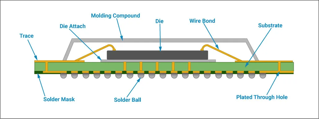
BGA is a surface-mount packaging technology where an IC is connected to a PCB via an array of solder balls arranged in a grid on the underside of the component. Unlike traditional pin-based packages like Pin Grid Arrays (PGAs) or Quad Flat Packages (QFPs), BGAs use solder balls (typically 0.3-0.75 mm in diameter) to establish electrical and mechanical connections. This allows for higher pin counts - often exceeding 1000 connections - while maintaining a small footprint, making BGAs ideal for applications like microprocessors, FPGAs, and memory chips in smartphones, laptops, and servers.
Why BGAs Matter
- High Density: BGAs support hundreds of connections in a compact space, enabling complex designs.
- Improved Electrical Performance: Shorter interconnects reduce inductance, minimizing signal distortion at high frequencies (e.g., up to 30 GHz in RF applications).
- Better Thermal Management: Solder balls dissipate heat more efficiently than traditional leads, with thermal resistance often as low as 10-20°C/W for plastic BGAs.
Key Challenges in BGA Assembly
BGA assembly is a sophisticated process that demands precision at every step. Below, we outline the primary challenges engineers face and why they matter.
1. Solder Joint Reliability
The quality of solder joints is critical to BGA performance. Improper reflow profiles can lead to defects like voids, cold joints, or solder bridging. For instance, a void occupying more than 25% of a solder joint's area can compromise electrical conductivity and thermal dissipation, leading to failures in high-power applications (e.g., 50 W processors). Additionally, lead-free solders, mandated by RoHS directives, have lower ductility, increasing the risk of joint fractures under thermal or mechanical stress.
2. Component Alignment
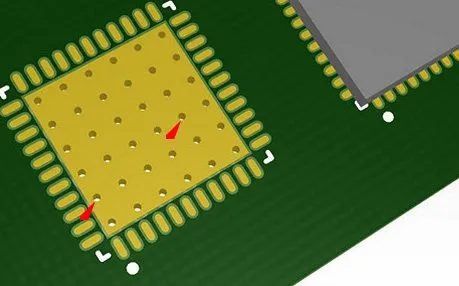
Precise alignment of BGA components is essential, as even a 0.1 mm misalignment can cause open circuits or shorts. The dense pin layout (e.g., 0.4-1.27 mm pitch) leaves little room for error, and automated pick-and-place machines must maintain placement accuracy within ±0.05 mm. Misalignment is particularly problematic for fine-pitch BGAs (≤0.5 mm), where traditional fan-out routing like dog-bone patterns becomes infeasible.
3. Inspection Difficulties
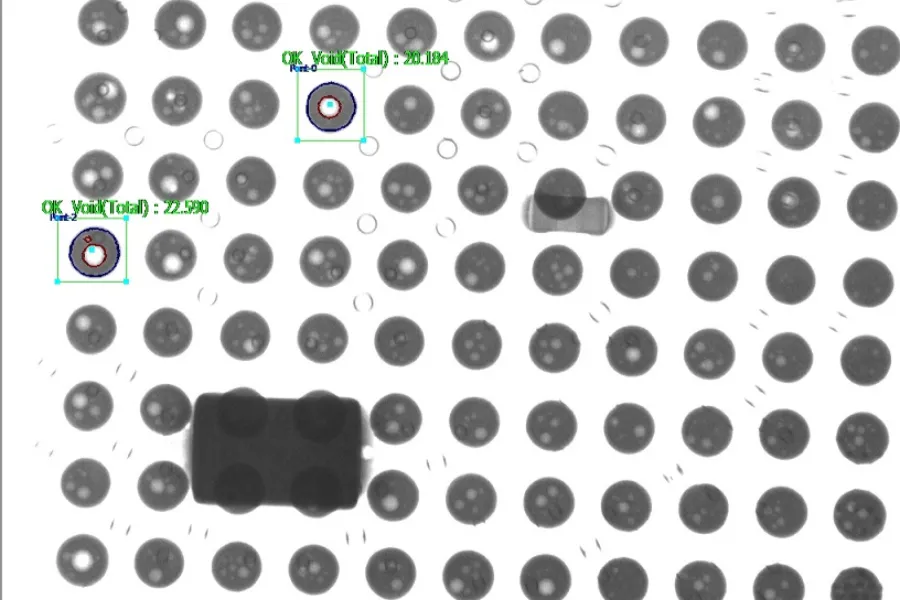
Unlike traditional surface-mount components, BGA solder joints are hidden beneath the package, making visual inspection impossible without specialized equipment. Automated Optical Inspection AOI systems struggle to detect subsurface defects, necessitating costly X-ray inspection systems to identify issues like voids or incomplete reflow. For example, X-ray systems can detect solder joint anomalies with resolutions down to 5 µm, but their high cost can strain budgets for smaller manufacturers.
4. Thermal Management
BGAs in high-power applications generate significant heat, requiring careful thermal management. Excessive temperatures during reflow (e.g., >260°C for lead-free solder) can damage components or cause thermal runaway, where solder joints weaken due to uneven heating. Additionally, mismatched coefficients of thermal expansion (CTE) between the PCB substrate (e.g., FR4 with CTE of 14-17 ppm/°C) and ceramic BGA packages (CTE of 6-8 ppm/°C) can lead to solder joint fractures over time.
5. Routing Complexity
Routing high-pin-count BGAs, such as those with 256-1000 pins, demands careful planning. Escape routing - connecting BGA pads to other PCB layers - often requires High-Density Interconnect (HDI) designs with microvias (≤0.15 mm diameter) and trace widths as narrow as 0.076 mm. Improper routing can increase signal noise, with crosstalk potentially exceeding 10% of signal amplitude in high-speed designs (e.g., 3-5 GHz).
Best Practices for Successful BGA Assembly
To overcome these challenges, engineers can adopt the following best practices, which we've refined through years of experience in PCB manufacturing and assembly.
1. Optimize PCB Design for BGA
- Use Non-Solder-Mask-Defined (NSMD) Pads: NSMD pads, where the solder mask does not overlap the copper pad, are preferred for pitches ≥0.5 mm. They provide better solder joint strength and reduce the risk of solder mask misalignment (typically ±0.1 mm). For ultra-fine pitches (≤0.5 mm), consider via-in-pad technology to maximize routing space.
- Incorporate Thermal Vias: Place thermal vias (0.2-0.3 mm diameter) under BGA packages to enhance heat dissipation. For high-power BGAs, aim for a via density of 4-6 vias/cm² to maintain thermal resistance below 15°C/W.
- Plan Escape Routing Early: Start BGA placement before other components to optimize trace routing. Use HDI layers (e.g., 6-12 layers) and microvias to reduce trace lengths, keeping impedance controlled at 50 ± 10% Ω for high-speed signals.
2. Perfect the Solder Paste Application
- Use Circular Stencil Apertures: Circular apertures (100-150 µm diameter) ensure uniform solder paste deposition on round BGA pads. Avoid square apertures, which can cause uneven paste application and increase voiding risk by up to 15%.
- Control Stencil Thickness: A stencil thickness of 0.1-0.15 mm balances paste volume for fine-pitch BGAs. For example, a 0.125 mm stencil with a 0.4 mm pitch BGA achieves a paste volume of approximately 0.002 mm³ per pad.
- Verify Paste Quality: Use high-quality, lead-free solder paste with a consistent particle size (e.g., Type 4, 20-38 µm) to minimize defects like bridging or insufficient solder.

3. Master the Reflow Process
- Optimize Reflow Profiles: Maintain a peak reflow temperature of 235-250°C for lead-free solder, with a time above liquidus (217°C) of 45-90 seconds to ensure complete melting without overheating. A ramp rate of 1-3°C/s prevents thermal shock to components.
- Use Nitrogen Atmosphere: Reflow in a nitrogen environment to reduce oxidation, lowering void formation by up to 20% compared to air-based reflow.
- Monitor Thermal Uniformity: Use thermocouples to ensure temperature uniformity across the PCB, keeping variations within ±5°C to avoid cold joints or component damage.
4. Leverage Advanced Inspection Techniques
- Invest in X-ray Inspection: Automated X-ray Inspection (AXI) systems are critical for detecting hidden defects like voids or incomplete reflow. Aim for a void rate below 10% of solder joint area for optimal reliability.
- Supplement with AOI: Use AOI for surface-level checks, such as component alignment or solder paste residue, to catch defects early and reduce X-ray inspection costs.
- Perform Boundary Scan Testing: For high-pin-count BGAs, use IEEE 1149.1 JTAG testing to verify electrical connectivity without physical probing, reducing test time by up to 30%.
5. Enhance Thermal and Mechanical Reliability
- Match CTEs: Select PCB substrates (e.g., FR4 or polyimide) with CTEs closely matching the BGA package to minimize thermal stress. For ceramic BGAs, low-CTE substrates like Isola 370HR (CTE ~14 ppm/°C) are ideal.
- Use Compliant Layers: Incorporate compliant layers in BGA packages to allow solder balls to flex slightly, reducing mechanical stress from vibration or thermal cycling. This is critical for applications like automotive or aerospace, where vibration levels can reach 10-20 G.
- Reinforce with Underfill: Apply epoxy underfill to BGA packages post-reflow to enhance mechanical stability, reducing solder joint failure rates by up to 40% in high-stress environments.
How ALLPCB Supports BGA Assembly Success
At ALLPCB, we understand the complexities of BGA assembly and are committed to helping engineers achieve reliable, high-performance PCBs. Our advanced manufacturing capabilities, including quick-turn prototyping (as fast as 24 hours), support for HDI designs with microvias, and state-of-the-art X-ray inspection, ensure precision and quality at every step. With global logistics and a robust supply chain, we streamline the production process, delivering fully assembled PCBs in as little as 5 days. Whether you're tackling fine-pitch BGAs or high-power applications, our expertise and cutting-edge equipment empower you to overcome assembly challenges with confidence.
Conclusion
BGA assembly is a cornerstone of modern electronics, enabling compact, high-performance designs but presenting significant challenges in design, soldering, inspection, and thermal management. By adopting best practices - such as optimized PCB layouts, precise solder paste application, controlled reflow profiles, and advanced inspection techniques - engineers can ensure reliable and efficient BGA assemblies. With careful planning and the right manufacturing partner, the complexities of BGA technology become opportunities to push the boundaries of innovation in electronics.


