 ALLPCB


In the fast-paced world of PCB manufacturing, ensuring precise component alignment is critical to producing high-quality boards. Automated Optical Inspection (AOI) plays a vital role in achieving this by detecting alignment issues and other defects with unmatched accuracy. If you're looking for insights on AOI setup for component alignment, AOI defect detection, AOI programming, or AOI system calibration, you've come to the right place. This guide offers a detailed look into how AOI systems work to ensure component alignment and overall board quality, providing actionable steps and practical tips for manufacturers and engineers.
At ALLPCB, we understand the importance of precision and efficiency in PCB production. This comprehensive guide will walk you through the essentials of AOI, from setup to calibration, helping you optimize your processes and reduce errors in component placement.
What Is Automated Optical Inspection (AOI) and Why Does It Matter for Component Alignment?
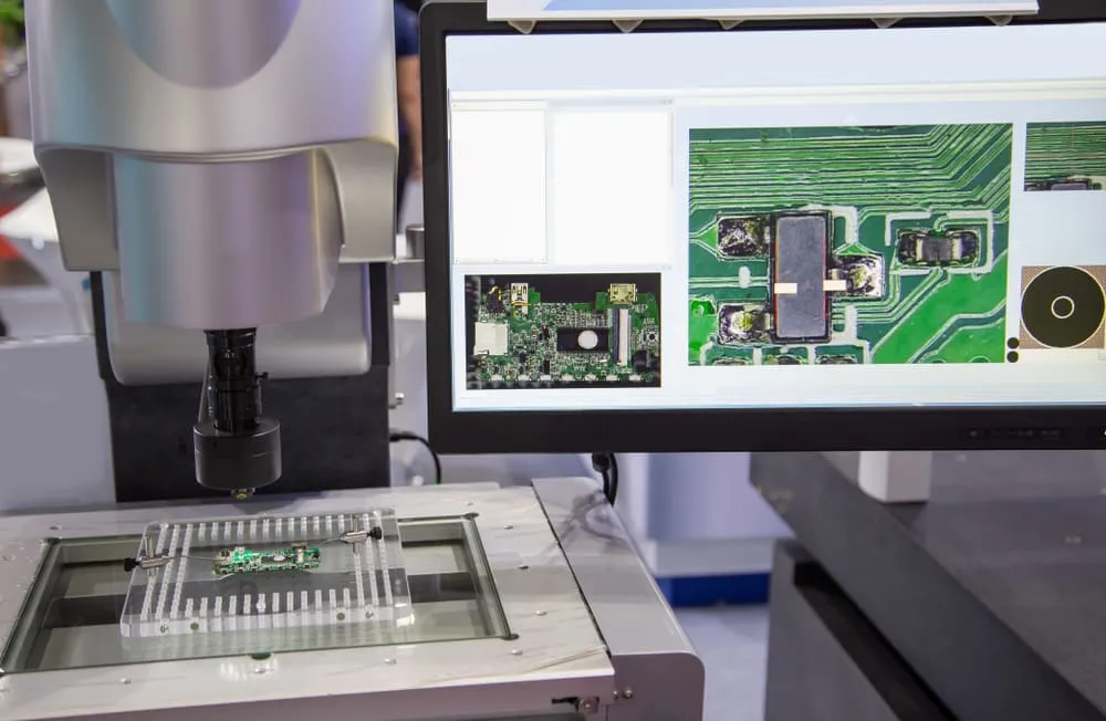
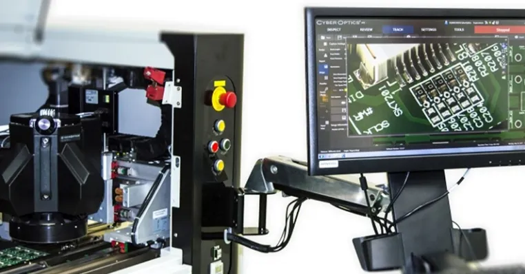
Automated Optical Inspection, or AOI, is a technology used in PCB manufacturing to visually inspect boards for defects and ensure quality. Using high-resolution cameras, advanced lighting, and sophisticated software, AOI systems scan PCBs to identify issues like misaligned components, missing parts, soldering defects, and more. When it comes to component alignment, AOI is indispensable because even a slight misalignment can lead to poor electrical connections, signal interference, or complete board failure.
In modern PCB designs, components are often incredibly small—sometimes as tiny as 01005 packages (0.4mm x 0.2mm). Manually inspecting such minuscule parts for alignment is nearly impossible. AOI systems, however, can achieve sub-pixel accuracy, detecting deviations as small as a few micrometers. This precision ensures that every component sits exactly where it should, maintaining the integrity of the board's design and functionality.
The Role of AOI in Component Alignment and Defect Detection
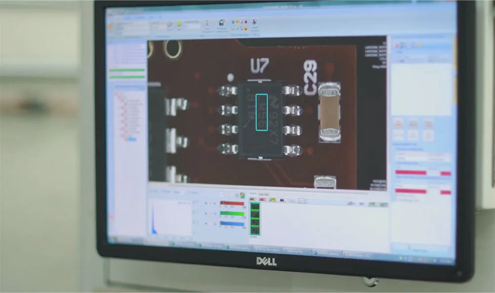
Component alignment is one of the most critical aspects of PCB assembly. Misaligned components can cause short circuits, open connections, or signal delays, leading to costly rework or product failures. AOI systems address this by comparing the actual placement of components against the intended design data, often sourced from Gerber files or CAD layouts. If a component is shifted by even 10 micrometers beyond the acceptable tolerance, the AOI system flags it as a defect.
Beyond alignment, AOI defect detection covers a wide range of issues, including:
- Missing Components: Identifying empty spots where parts should be placed.
- Incorrect Polarity: Detecting components installed with the wrong orientation, which can disrupt circuit functionality.
- Soldering Issues: Spotting insufficient solder, bridges, or cold joints that affect connectivity.
- Physical Damage: Noticing scratches, cracks, or other surface defects on components or the board itself.
By catching these issues early in the manufacturing process, AOI reduces the risk of defective boards reaching the end user, saving time and resources while boosting overall quality.
Step-by-Step Guide to AOI Setup for Component Alignment
Setting up an AOI system for component alignment requires careful planning and attention to detail. Here's a step-by-step breakdown of the AOI setup for component alignment to help you get started:
1. Prepare the Design Data
Begin by uploading the PCB design files into the AOI system. These files typically include Gerber data, BOM (Bill of Materials), and CAD layouts. The system uses this information as a reference to compare the physical board against the intended design. Ensure that the data is accurate and up-to-date to avoid false positives during inspection.
2. Configure the Inspection Area
Define the specific areas of the PCB that need inspection. For component alignment, focus on high-density zones where small parts are placed close together. Adjust the field of view (FOV) of the cameras to cover these areas with sufficient resolution—often around 5 to 10 micrometers per pixel for tiny components.
3. Set Alignment Tolerances
Specify the acceptable tolerance levels for component placement. For instance, a common tolerance for standard components might be ±50 micrometers in the X and Y directions. However, for ultra-small parts, you might tighten this to ±20 micrometers. Setting precise thresholds ensures the AOI system flags only genuine alignment issues.
4. Test and Validate
Run a test batch of PCBs through the AOI system to verify the setup. Check if the system correctly identifies misaligned components and other defects. If you notice false positives or missed defects, adjust the parameters and repeat the test until the results are reliable.
Related Reading: Automated Optical Inspection (AOI): Ensuring Quality in PCB Assembly
Mastering AOI Programming for Optimal Results
AOI programming is the backbone of an effective inspection process. Programming involves creating rules and algorithms that guide the AOI system in identifying defects and verifying alignment. Here's how to approach programming for component alignment:
1. Define Inspection Criteria
Program the system to recognize specific defects related to alignment. This includes setting thresholds for positional deviations, rotation errors, and component height. For example, if a component's rotation exceeds 5 degrees from the intended angle, the system should flag it as a defect.
2. Utilize Pattern Matching
Most AOI systems use pattern-matching algorithms to compare the scanned image of the PCB with a "golden" reference image or design data. Program the system to focus on key features of each component, such as edges or markings, to ensure accurate alignment detection.
3. Incorporate Machine Learning
Advanced AOI systems leverage artificial intelligence (AI) and machine learning to improve defect detection over time. By programming the system to learn from past inspections, you can reduce false positives and enhance accuracy, especially for complex boards with varied components.
4. Regularly Update Programs
As PCB designs evolve, so must your AOI programming. Update the inspection criteria and algorithms whenever there are changes in component types, board layouts, or manufacturing processes. This ensures the system remains effective in detecting alignment issues.
The Importance of AOI System Calibration
AOI system calibration is a critical step to ensure the accuracy and reliability of inspections. Without proper calibration, even the most advanced AOI system can produce incorrect results, leading to missed defects or unnecessary rework. Here's how to approach calibration for component alignment:
1. Calibrate Camera and Lighting
The cameras and lighting are the heart of any AOI system. Calibrate the cameras to achieve consistent focus and resolution across the entire inspection area. Ensure the lighting is uniform—often a combination of top, side, and coaxial lighting—to highlight component edges and surfaces without creating shadows or glare. For instance, a brightness level of 80-100 lumens per square inch is often ideal for inspecting small components.
2. Verify Positional Accuracy
Use a calibration board with known reference points to test the system's positional accuracy. The AOI should detect these points within a tolerance of ±5 micrometers. If the system shows deviations, adjust the camera alignment or software settings until the accuracy meets the required standard.
3. Check Software Algorithms
Calibration isn't just about hardware; the software must also be fine-tuned. Run a series of test inspections on boards with known defects to ensure the algorithms correctly identify alignment issues. If the system misses defects or flags non-issues, recalibrate the detection thresholds.
4. Schedule Regular Maintenance
Calibration isn't a one-time task. Schedule regular maintenance checks—ideally every 3 to 6 months or after 10,000 inspections—to ensure the system remains accurate. Environmental factors like temperature changes or vibrations can affect calibration over time, so consistent monitoring is essential.
Benefits of Using AOI for Component Alignment in PCB Manufacturing
Implementing AOI for component alignment offers numerous advantages that directly impact the quality and efficiency of PCB production:
- Enhanced Accuracy: AOI systems detect alignment issues with precision down to a few micrometers, far surpassing manual inspection capabilities.
- Time Efficiency: Automated inspections can process hundreds of boards per hour, significantly speeding up quality control compared to human inspectors.
- Cost Savings: By catching alignment defects early, AOI reduces the need for costly rework or scrap, saving resources in the long run.
- Consistency: Unlike manual inspections, which can vary based on the inspector's experience or fatigue, AOI provides consistent results every time.
- Data Insights: AOI systems generate detailed reports on defect trends, helping manufacturers identify and address recurring alignment issues in their processes.
Related Reading: Automated Optical Inspection (AOI) Strategies for Maximizing Quality in PCB Mass Production
Challenges and Solutions in AOI for Component Alignment
While AOI is a powerful tool, it’s not without challenges. Here are some common issues related to component alignment and how to overcome them:
Challenge 1: False Positives
Sometimes, AOI systems flag non-issues as defects, slowing down production. This often happens due to overly strict tolerances or poor lighting conditions. To solve this, fine-tune the inspection parameters and ensure optimal lighting setups during calibration.
Challenge 2: Complex Board Designs
High-density boards with overlapping components or reflective surfaces can confuse AOI systems. Use advanced multi-angle cameras and programmable lighting to capture clear images from different perspectives, improving detection accuracy.
Challenge 3: Small Component Detection
Tiny components like 01005 packages are harder to inspect due to their size. Invest in high-resolution cameras with at least 5-micrometer pixel resolution and program the system to focus on specific features of these small parts for accurate alignment checks.
Future Trends in AOI for Component Alignment
The field of AOI is evolving rapidly, driven by advancements in technology. Here are some trends to watch for in component alignment inspection:
- AI Integration: Artificial intelligence is enhancing AOI systems by enabling adaptive learning. Systems can now analyze past data to predict and prevent alignment issues before they occur.
- 3D Inspection: Traditional 2D AOI is being supplemented by 3D inspection technologies that measure component height and tilt, providing a more comprehensive view of alignment.
- Industry 4.0 Connectivity: AOI systems are increasingly integrated into smart manufacturing setups, allowing real-time data sharing with other equipment for immediate process adjustments.
Conclusion: Elevate Your PCB Quality with AOI for Component Alignment
Automated Optical Inspection is a game-changer for ensuring precise component alignment in PCB manufacturing. From AOI setup for component alignment to AOI defect detection, AOI programming, and AOI system calibration, mastering these aspects can significantly improve the quality and reliability of your boards. By following the steps and best practices outlined in this guide, you can optimize your AOI processes to catch alignment issues early, reduce defects, and streamline production.
At ALLPCB, we’re committed to supporting manufacturers with cutting-edge solutions for PCB assembly and inspection. Implementing AOI for component alignment not only enhances product quality but also boosts efficiency, ensuring your boards meet the highest standards. Embrace this technology to stay ahead in the competitive world of electronics manufacturing.


