ALLPCB


If you're diving into PCB design, you might be wondering how through-hole vias and Design for Manufacturability (DFM) work together to create reliable, cost-effective circuit boards. Simply put, through-hole vias are essential for connecting different layers of a PCB, while DFM ensures your design can be manufactured efficiently without errors or delays. In this blog, we'll explore the role of through-hole vias, key via design rules, and how DFM principles can streamline PCB manufacturing. Let’s break it down step by step to help you design better boards with practical tips and insights.
What Are Through-Hole Vias in PCB Design?
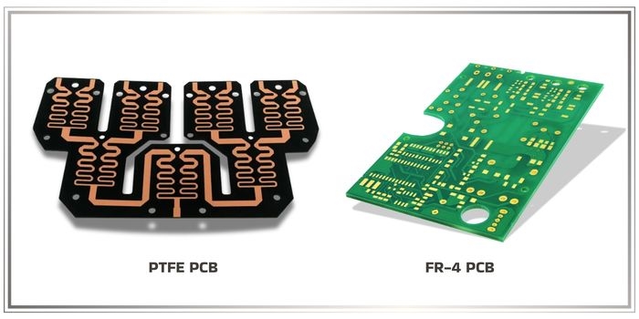
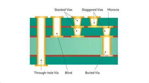
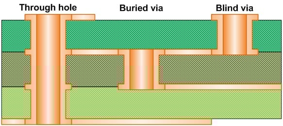
Through-hole vias are small, conductive holes drilled through a printed circuit board (PCB) to connect different layers. Unlike blind or buried vias, which only connect specific layers, through-hole vias go all the way from the top to the bottom of the board. They’re often plated with copper to ensure a solid electrical connection. These vias are critical for routing signals, power, and ground between layers, especially in multi-layer PCBs.
In terms of manufacturing, through-hole vias are one of the most common types used due to their simplicity and reliability. They’re also easier to inspect and repair compared to other via types. However, their design and placement can significantly impact the manufacturability of a PCB, which is where DFM comes into play.
Why Design for Manufacturability (DFM) Matters in PCB Design
Design for Manufacturability, or DFM, is a set of guidelines and practices aimed at making your PCB design easier and more cost-effective to produce. When applied correctly, DFM reduces errors, lowers production costs, and speeds up the manufacturing process. For engineers, focusing on PCB design for manufacturability means fewer revisions, less waste, and a smoother transition from prototype to mass production.
DFM is especially important when working with through-hole vias because poor via design can lead to issues like insufficient copper plating, weak solder joints, or even board failure during assembly. By following DFM principles, you can avoid these pitfalls and ensure your design meets manufacturing capabilities.
Key Via Design Rules for Through-Hole Vias
To achieve a manufacturable PCB design, you need to follow specific via design rules. These guidelines help ensure that through-hole vias are placed and sized correctly for both functionality and production. Here are some critical rules to keep in mind:
1. Via Size and Aspect Ratio
The size of a through-hole via, including its diameter and the thickness of the board it passes through, is crucial. A common rule of thumb is to maintain an aspect ratio (board thickness to via diameter) of no more than 8:1. For example, on a 1.6mm thick board, the via diameter should be at least 0.2mm. If the aspect ratio is too high, it becomes difficult to plate the via with copper evenly, leading to weak connections.
Smaller vias save space but can be harder to manufacture. Most standard fabrication processes can handle vias with a minimum diameter of 0.3mm, but always check with your manufacturing partner for their specific capabilities.
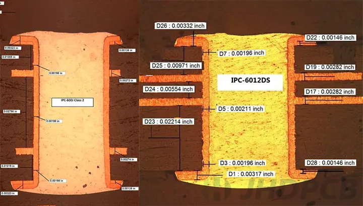
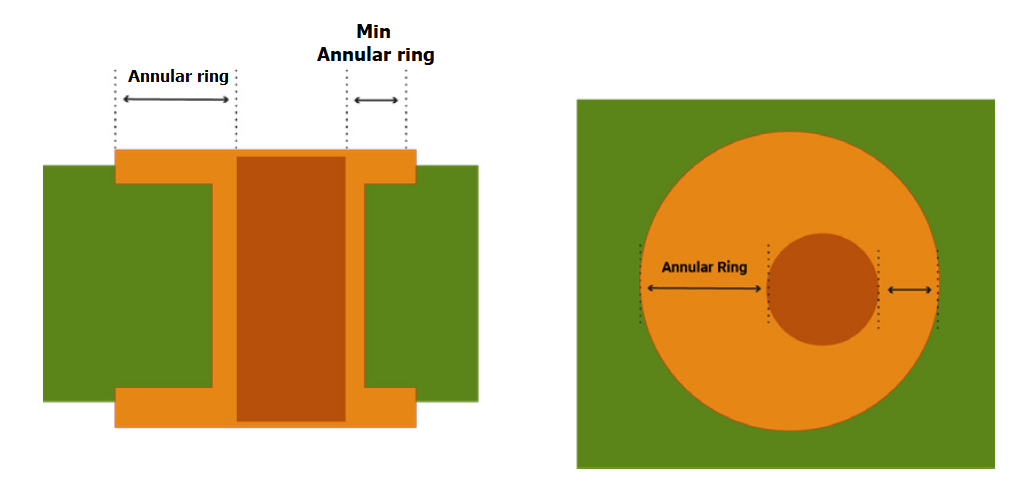
2. Annular Ring Dimensions
The annular ring is the copper pad surrounding the via hole. It provides a surface for soldering and ensures a strong connection. According to IPC-2221 standards, the minimum annular ring width should be at least 0.2mm for external layers to account for manufacturing tolerances. A smaller annular ring risks breaking during drilling or assembly, leading to defective boards.
3. Via Spacing and Placement
Vias need to be spaced adequately to avoid interference with other components or traces. A general guideline is to keep vias at least 0.5mm apart from each other and from component pads. Placing vias too close together can cause short circuits or make soldering difficult. Additionally, avoid placing vias under components unless absolutely necessary, as this can complicate assembly and inspection.
4. Via Filling and Plating
Through-hole vias are typically plated with copper to ensure conductivity, but in some cases, they may be filled with conductive or non-conductive materials to improve strength or thermal performance. For high-current applications, ensure the copper plating thickness is at least 25 micrometers (1 mil) to handle the load without overheating. Poor plating can lead to open circuits or increased resistance.
How DFM Enhances Through-Hole Via Design
Integrating DFM into your PCB design process ensures that through-hole vias don’t become a bottleneck during manufacturing. Here’s how DFM principles directly improve via design and overall board production:
1. Simplifying Fabrication with Standard Sizes
DFM encourages the use of standard via sizes and drill bits to avoid custom tooling, which can increase costs and lead times. For instance, sticking to common via diameters like 0.3mm or 0.4mm ensures that manufacturers can use readily available equipment, reducing the risk of errors during drilling.
2. Reducing Thermal and Mechanical Stress
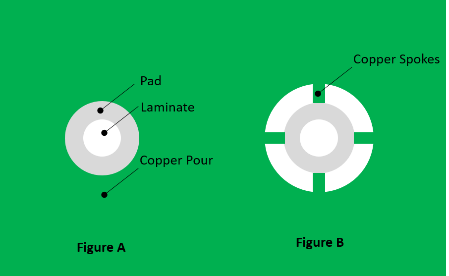
Through-hole vias can create stress points on a PCB, especially during thermal cycling or mechanical handling. DFM practices recommend placing vias away from board edges (at least 2mm) to prevent cracking. Additionally, using thermal relief pads for vias connected to power or ground planes can minimize heat buildup during soldering, protecting the board and components.
3. Optimizing for Assembly
During assembly, through-hole vias often serve as mounting points for components or connectors. DFM suggests aligning via locations with component leads to simplify soldering and reduce manual labor. For automated assembly, ensure that vias are not placed in areas that could interfere with pick-and-place machines or wave soldering equipment.
Common Challenges with Through-Hole Vias and DFM Solutions
Even with careful planning, issues can arise when designing with through-hole vias. Here are some common challenges and how DFM can help address them:
1. Signal Integrity Issues
In high-speed designs, through-hole vias can act as stubs, causing signal reflections and degrading performance. For example, in a design operating at 5 GHz, an improperly sized via stub could introduce a delay of several picoseconds, leading to data errors. DFM recommends minimizing via length and using back-drilling techniques to remove unused portions of the via, improving signal integrity.
2. Manufacturing Defects
Defects like incomplete copper plating or misaligned drilling can compromise via reliability. DFM emphasizes early collaboration with your manufacturer to understand their process limits, such as minimum drill size or plating thickness. Performing a design review before fabrication can catch potential issues, saving time and cost.
3. Cost Overruns
Complex via designs, such as those requiring microvias or non-standard sizes, can drive up production costs. A DFM approach focuses on simplifying the design wherever possible, such as using fewer via types or consolidating connections to reduce layer count. For instance, reducing a board from 6 layers to 4 by optimizing via placement could cut fabrication costs by up to 20%.
Practical Tips for PCB Manufacturing with Through-Hole Vias
To wrap up the actionable advice, here are some practical tips for ensuring your PCB design for manufacturability is on point when using through-hole vias:
- Use Design Software Tools: Leverage PCB design software with built-in DFM checks to automatically flag issues like insufficient annular rings or improper via spacing.
- Consult Manufacturer Guidelines: Every manufacturer has specific capabilities and limits. Request their DFM guidelines before finalizing your design to avoid surprises during production.
- Test Prototypes: Before moving to mass production, build and test a prototype to verify that your via design performs as expected under real-world conditions.
- Balance Density and Manufacturability: While dense designs save space, they can complicate manufacturing. Aim for a balance by spacing vias and components reasonably.
Benefits of Combining Through-Hole Vias with DFM
When you pair thoughtful via design with DFM principles, the benefits are clear. First, you’ll see improved reliability, as well-designed vias reduce the risk of electrical failures or mechanical damage. Second, production costs drop because DFM minimizes errors and the need for rework. Finally, your time-to-market shortens since a manufacturable design moves through fabrication and assembly faster.
For example, a study of PCB production cycles showed that designs adhering to DFM guidelines reduced manufacturing defects by up to 30%, saving thousands of dollars in rework costs for mid-volume runs. These savings and efficiency gains make DFM a must for any serious PCB project.
Conclusion
Through-hole vias are a fundamental part of PCB design, enabling connections across layers for reliable electrical performance. However, their design must align with Design for Manufacturability (DFM) principles to ensure smooth and cost-effective PCB manufacturing. By following via design rules—such as maintaining proper aspect ratios, annular ring sizes, and spacing—you can avoid common pitfalls. Additionally, integrating DFM practices like using standard sizes, optimizing placement, and collaborating with manufacturers helps streamline production and reduce costs.
Whether you’re a seasoned engineer or just starting out, focusing on PCB design for manufacturability with through-hole vias will elevate the quality of your boards. Keep these guidelines and tips in mind for your next project, and you’ll be well on your way to creating efficient, reliable, and production-ready designs.