ALLPCB


Thermal management during soldering remains a critical consideration in printed circuit board assembly. Large copper areas such as ground or power planes can act as heat sinks, drawing heat away from component pads and resulting in incomplete solder joints. Thermal relief patterns address this issue by restricting the thermal path between a pad and its connected copper pour while preserving electrical continuity. Proper implementation ensures reliable solderability without compromising signal integrity or current-carrying capacity. Engineers routinely evaluate these patterns during layout to meet both manufacturing and performance requirements.
What Is Thermal Relief and Why It Matters
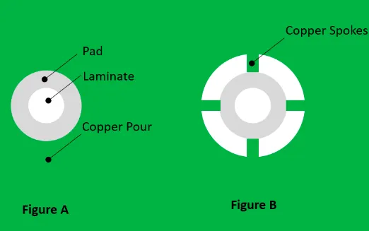
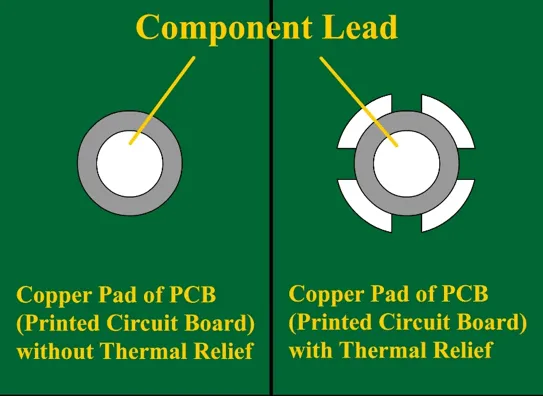
Thermal relief consists of narrow copper spokes or bridges that connect a pad to a surrounding copper plane. These spokes reduce the rate of heat transfer during reflow or wave soldering, allowing the pad to reach the necessary temperature for proper solder wetting. Without relief, pads attached to extensive copper areas often remain cooler than adjacent lands, leading to dull or insufficient solder fillets. Industry standards such as IPC-2221 establish design guidelines that help balance thermal, electrical, and mechanical needs. Effective thermal relief improves first-pass yield and reduces rework associated with cold solder joints.
Technical Principles and Mechanisms
Heat flow follows the path of least thermal resistance. A direct connection between a pad and a large copper plane creates a low-resistance thermal path, causing rapid heat dissipation into the plane. Introducing spokes of controlled width and length increases thermal resistance while maintaining low electrical resistance. The number of spokes, their angular spacing, and their width directly influence both thermal isolation and current capacity. IPC-6012E outlines acceptance criteria for copper features that ensure mechanical integrity after thermal cycling. Designers must verify that spoke dimensions satisfy both thermal and current-density requirements under expected operating conditions.
Practical Solutions and Best Practices
Begin by defining thermal relief parameters within the design rules for copper pours. Set spoke width, spoke count, and air-gap clearance to values that achieve the desired thermal isolation without violating minimum conductor width rules. For most through-hole and surface-mount pads connected to planes, four spokes spaced at ninety degrees provide a practical balance. Adjust spoke width according to current requirements; narrower spokes improve thermal relief but limit maximum current before excessive voltage drop occurs. Review the resulting pad geometry in the layout viewer to confirm that spokes do not create unintended impedance discontinuities or manufacturing issues.
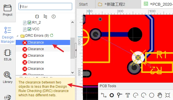
Custom thermal relief pads can be created when standard settings do not meet specific electrical or thermal targets. Draw the pad outline and manually add copper spokes using the appropriate polygon or track tools, ensuring each spoke maintains electrical connectivity to the plane. Verify that the custom geometry complies with minimum annular ring and clearance rules. After placement, run a design rule check focused on thermal relief parameters to identify any violations before generating manufacturing outputs.
Related Reading: Copper Pour and Thermal Relief: A Guide to Preventing Soldering Issues
Troubleshooting Common Issues
When solder joints appear incomplete despite thermal relief, examine spoke width and count first. Excessively wide spokes can still conduct too much heat; reducing width by 0.2–0.3 mm often restores proper wetting. Conversely, spokes that are too narrow may violate current-carrying requirements and should be widened or supplemented with additional thermal vias placed outside the pad area. Inspect the copper pour for unintended connections that bypass the intended relief pattern. Re-running the thermal relief update command after any plane modification ensures consistency across the board.
Related Reading: SMT Pad Thermal Relief: Preventing Tombstoning and Ensuring Reliable Soldering
Conclusion
Thermal relief implementation directly affects soldering quality and long-term reliability of printed circuit boards. By configuring design rules appropriately, creating custom pads when needed, and verifying results through systematic checks, designers achieve consistent solder joints while preserving electrical performance. Adherence to established industry standards ensures that relief patterns meet both manufacturing and operational expectations. Regular review of thermal relief settings during the layout process minimizes costly iterations and supports high-yield production.
FAQs
Q1: How do Altium Designer thermal relief settings affect solder joint quality?
A1: Proper configuration of thermal relief parameters in Altium Designer limits heat flow from pads into copper planes, allowing pads to reach soldering temperature more uniformly. This results in complete solder fillets and reduced incidence of cold joints. Engineers adjust spoke width and count according to current requirements and manufacturing process capabilities.
Q2: What are the recommended thermal relief design rules in Altium for high-current applications?
A2: Thermal relief design rules in Altium should specify spoke widths that satisfy both thermal isolation and current density limits. Four spokes are commonly used, with width increased for higher currents while maintaining adequate air gaps. Verification through design rule checks ensures compliance before manufacturing data generation.
Q3: Can custom thermal relief pads in Altium improve performance over default settings?
A3: Custom thermal relief pads in Altium allow precise control of spoke geometry when standard options do not meet thermal or electrical targets. Designers create these pads by manually defining spoke dimensions and verifying connectivity to the plane. This approach supports optimized layouts for specialized applications.
Q4: Does Altium thermal simulation help validate thermal relief effectiveness?
A4: Altium thermal simulation tools enable evaluation of temperature distribution around pads with different relief patterns. Engineers can compare heat flow with and without relief spokes to confirm that chosen settings achieve the intended isolation. Simulation results guide final adjustments prior to fabrication.
References
IPC-2221: Generic Standard on Printed Board Design.
IPC-6012E: Qualification and Performance Specification for Rigid Printed Boards.
Altium Designer Documentation: Polygon Pours and Thermal Relief settings.