ALLPCB


Stencil aperture design plays a central role in surface mount technology assembly. The apertures in the stencil control the volume and shape of solder paste deposited onto printed circuit board pads. Proper design ensures consistent paste transfer, which directly influences the formation of reliable solder joints during reflow. Inadequate aperture sizing or geometry can lead to defects that compromise electrical and mechanical performance over the product lifecycle. Engineers must balance paste volume needs against release efficiency to achieve high yields in high-density boards.
Why Stencil Aperture Design Matters for Reliability
Stencil aperture design determines how much solder paste reaches each pad before components are placed and reflowed. The aperture dimensions, combined with stencil thickness, set the theoretical paste volume. Actual transferred volume depends on factors such as paste rheology, printing parameters, and aperture wall characteristics. When volume falls short or exceeds requirements, joints may form with insufficient fillet height or excessive material that promotes shorts. These variations affect long-term reliability under thermal cycling, vibration, and mechanical stress. Industry guidelines emphasize aperture optimization to maintain consistent deposition across production runs.
Solder joint reliability suffers when paste volume deviates from targets established for specific component types. Insufficient paste can produce weak or open joints, while excess paste increases the risk of bridging between adjacent pads. Both outcomes reduce first-pass yield and may require rework that introduces additional variables. Designers therefore apply stencil design rules early in the layout phase to align aperture parameters with pad geometry and component pitch. This proactive approach minimizes downstream assembly issues and supports compliance with established quality criteria.

Technical Principles of Aperture Design and Paste Transfer
Aperture design follows principles centered on area ratio and aspect ratio. The area ratio compares the aperture opening area to the sidewall surface area. Values below recommended thresholds reduce paste release efficiency because surface tension holds paste inside the aperture. The aspect ratio compares aperture width to stencil thickness and influences how cleanly paste separates from the stencil walls. Both metrics guide engineers in selecting aperture sizes that promote greater than 75 percent transfer efficiency for most applications.
Solder bridging occurs when excess paste flows between closely spaced pads during printing or reflow. Tombstoning arises when uneven paste volumes on opposite ends of a passive component create unbalanced surface tension forces that lift one side of the part. These defects trace directly to aperture dimensions that fail to match pad size or component requirements. Rectangular apertures with home-plate or other modified shapes can improve release for fine-pitch devices by reducing the contact area with the stencil walls. Engineers calculate expected paste volume using aperture area multiplied by stencil thickness, then adjust for expected transfer efficiency based on the chosen ratios.
Paste release also depends on aperture wall finish and stencil material. Laser-cut or electroformed apertures with smooth, tapered walls improve release compared with rougher surfaces. When area ratios drop too low, paste tends to remain in the aperture rather than transferring fully to the pad. This shortfall leaves joints with reduced solder volume that may not withstand thermal expansion mismatches between component and board. Structured evaluation of these mechanisms helps identify root causes of intermittent failures observed during reliability testing.

Best Practices for Stencil Aperture Optimization
Engineers begin optimization by reviewing component datasheets and land pattern recommendations to establish target paste volumes. Aperture dimensions are then sized as a percentage of pad dimensions, typically reduced for fine-pitch parts to prevent bridging while maintaining adequate volume. For many surface-mount devices, a 10 to 20 percent reduction relative to pad size provides a practical starting point, subject to verification through test prints. Area ratio targets above 0.66 and aspect ratios above 1.5 serve as common benchmarks for acceptable release performance.
Step stencils offer another optimization path when boards contain both standard and fine-pitch components. Thinner sections over dense areas limit paste volume locally, while thicker sections elsewhere supply sufficient material for larger pads. This approach reduces the need for multiple print passes or separate stencils. Aperture shapes receive attention as well. Rounded corners or modified geometries can enhance paste release without sacrificing volume on rectangular pads. Validation through solder paste inspection after printing confirms that actual deposited volumes fall within acceptable process windows before full production begins.
Related Reading: Advanced Stencil Aperture Designs for Optimized Solder Paste Deposition
Process parameters interact with aperture design. Squeegee pressure, speed, and angle must complement the chosen apertures to achieve clean fills and releases. Regular inspection of printed boards identifies trends such as incomplete aperture filling or tailing that signal the need for design adjustments. Iterative refinement based on measured volumes and defect rates refines the stencil layout for sustained high reliability.
Troubleshooting Common Defects Linked to Aperture Design
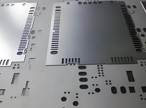
When bridging appears, engineers first examine whether apertures are oversized relative to pad spacing. Reducing aperture width or switching to segmented patterns for thermal pads often resolves the issue while preserving required volume. Tombstoning frequently points to asymmetric paste deposits caused by inconsistent aperture sizing across a component footprint. Matching aperture dimensions more precisely to pad geometry and verifying uniform stencil thickness corrects the imbalance.
Voiding under components such as quad flat no-lead packages can stem from large single apertures that trap volatiles. Segmented aperture patterns create channels for gas escape and lower void percentages. Engineers document defect locations and volumes during process audits to correlate specific aperture features with observed issues. Adjustments remain data-driven and avoid arbitrary changes that could introduce new variables.
Related Reading: The Art of SMT Stencil Aperture Design: Minimizing Defects and Maximizing Yield

Conclusion
Stencil aperture design exerts a direct and measurable influence on solder joint reliability through its control of paste volume and release characteristics. Attention to area ratio, aspect ratio, and geometry enables consistent deposition that supports robust fillet formation and minimizes defects such as bridging and tombstoning. Structured application of design principles, combined with process validation, yields assemblies that meet performance expectations under operational stresses. Engineers who integrate these considerations early achieve higher yields and more predictable long-term reliability.
FAQs
Q1: What role does stencil aperture design play in preventing solder bridging?
A1: Stencil aperture design controls the amount of solder paste deposited on adjacent pads. Oversized apertures relative to pad spacing allow excess paste to flow together during printing or reflow, creating bridges. Proper sizing and shape adjustments, guided by stencil design rules, limit volume while ensuring adequate material for each joint, thereby reducing bridging risk in dense layouts.
Q2: How does aperture optimization affect tombstoning in passive components?
A2: Aperture optimization ensures balanced paste volumes on both ends of chip resistors and capacitors. Uneven deposits from mismatched apertures create surface tension differences that cause one side to lift during reflow. Consistent aperture dimensions aligned with pad geometry promote even wetting and stable component placement throughout the soldering process.
Q3: Why are area ratio and aspect ratio important in stencil aperture design?
A3: Area ratio and aspect ratio determine how effectively solder paste releases from the stencil aperture onto the pad. Ratios that fall below established thresholds trap paste inside the aperture, resulting in insufficient volume for reliable joints. Maintaining recommended values supports high transfer efficiency and consistent solder joint formation across production volumes.
Q4: What considerations guide stencil aperture adjustments for fine-pitch components?
A4: Fine-pitch components require aperture reductions and sometimes modified shapes to prevent bridging while delivering enough paste. Engineers evaluate component pitch, pad dimensions, and stencil thickness together. Test printing and inspection verify that the chosen apertures achieve target volumes without introducing defects that compromise joint reliability.
References
IPC-7525B — Stencil Design Guidelines. IPC, 2011
J-STD-001 — Requirements for Soldered Electrical and Electronic Assemblies. IPC, 2020
IPC-A-610 — Acceptability of Electronic Assemblies. IPC, 2020