ALLPCB


Grounding forms the foundation of reliable PCB performance by providing a stable reference for all signals and power paths. Engineers recognize that effective grounding directly influences signal integrity and electromagnetic compatibility in modern electronic systems. Poor grounding practices often lead to unexpected noise coupling that degrades circuit operation. Structured approaches to grounding in schematics help maintain consistent voltage levels across the board. These methods become especially critical as operating frequencies increase and component densities rise.
Why Proper Grounding Matters in PCB Design
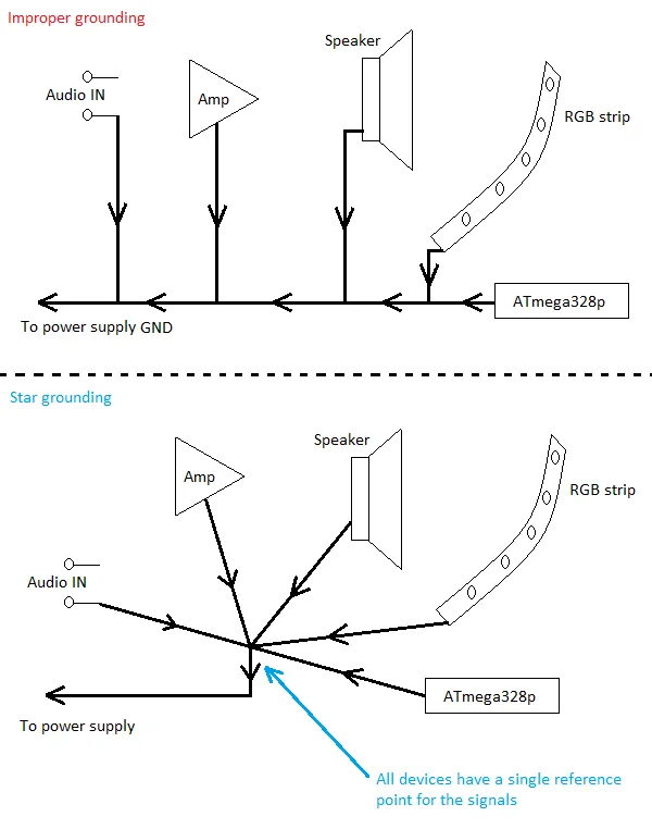
Grounding techniques in PCB schematics address the fundamental need to minimize voltage differences between various circuit sections. Noise and interference arise when return currents find unintended paths that create voltage drops or couple into sensitive signals. Star grounding PCB configurations separate analog and digital return paths to prevent cross-contamination of noise. Ground loops in PCB layouts occur when multiple ground connections form closed paths that act as antennas for electromagnetic fields. Minimizing interference PCB designs requires careful planning of ground topology from the schematic stage onward. Engineers apply these principles to ensure stable operation in mixed-signal environments where small voltage fluctuations can corrupt data.
Technical Principles Behind Noise and Interference
Current flow through ground conductors generates voltage according to basic Ohm's law relationships. When return paths share common impedance, switching currents from digital sections induce noise on analog references. Ground loops in PCB structures amplify this effect by enclosing areas that capture external magnetic fields. The resulting induced voltages appear as differential signals at input stages. Star grounding PCB methods reduce shared impedance by routing each functional block to a common point. This topology limits the formation of large current loops that radiate or receive interference. Signal return paths must remain as short and direct as possible to keep loop areas minimal. High-frequency components demand additional consideration of parasitic inductance and capacitance along ground traces.
Related Reading: PCB Grounding Techniques: A Guide to Minimizing Noise and Ensuring Reliable Connections
Mechanisms of Noise Coupling in Ground Systems
Electromagnetic interference enters circuits through conductive, capacitive, and inductive mechanisms tied directly to ground integrity. Conductive coupling occurs when noise currents travel along shared ground conductors between sections. Capacitive coupling arises from electric fields between adjacent traces and ground planes when separation distances vary. Inductive coupling results from changing magnetic fields linking ground loops in PCB assemblies. Engineers analyze these paths by modeling ground as a network of resistances and inductances rather than an ideal zero-voltage node. Separation of analog and digital grounds at the schematic level interrupts these coupling routes before layout begins. Proper partitioning ensures that high-current digital returns do not flow through low-level analog ground areas.
Related Reading: Techniques to minimize noise coupling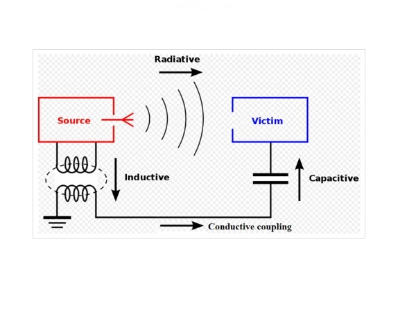
Best Practices for Implementing Grounding Techniques
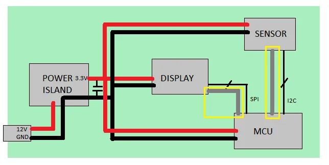
Schematic development begins with defining distinct ground symbols for analog, digital, and power sections. These symbols connect to a single star point that serves as the system reference. PCB grounding techniques schematic documentation includes clear notes on connection hierarchy and return current directions. Ground planes in multilayer boards provide low-impedance paths when properly tied to the star point through vias. Engineers place decoupling capacitors close to power pins and route their returns directly to the local ground plane. Analog circuits receive dedicated ground traces that meet the main ground only at the designated star location. Testing at the prototype stage verifies that noise levels remain within acceptable limits after these connections are established.
Troubleshooting Common Grounding Issues
When noise appears in measurements, engineers first examine ground connections for unintended multiple paths. Ground loops in PCB designs often manifest as 50 or 60 hertz hum in audio circuits or baseline wander in sensor outputs. Star grounding PCB revisions typically resolve these problems by consolidating returns. Additional shielding or guard traces may supplement grounding when external fields remain problematic. Systematic measurement of voltage differences between ground points confirms whether the reference remains stable under load. Documentation of each change ensures repeatability across design iterations.
Conclusion
Effective grounding in PCB schematics reduces noise and interference by controlling return current paths and minimizing loop areas. Star grounding PCB approaches combined with careful separation of functional grounds deliver measurable improvements in signal quality. Engineers who apply these principles from the schematic stage achieve more predictable performance in final assemblies. Consistent attention to ground topology supports compliance with electromagnetic compatibility requirements while maintaining design flexibility.
FAQs
Q1: What are the main PCB grounding techniques schematic methods used to reduce noise?
A1: Engineers employ star grounding, ground plane partitioning, and separate analog-digital returns as primary PCB grounding techniques schematic approaches. These methods limit shared impedance and prevent noise from digital switching from reaching sensitive analog sections. Proper implementation keeps return currents localized and reduces overall interference levels.
Q2: How does star grounding PCB configuration help with ground loops in PCB layouts?
A2: Star grounding PCB topology connects each circuit block to a single common point, eliminating multiple paths that would otherwise form ground loops in PCB structures. This arrangement ensures that currents from different sections do not share conductors except at the reference node. The result is lower induced noise and improved measurement accuracy.
Q3: Why is minimizing interference PCB important during the schematic phase?
A3: Minimizing interference PCB begins at the schematic stage because ground topology decisions made early determine the feasibility of clean layouts later. Early identification of return paths allows designers to allocate layers and place components to support low-impedance grounding. This proactive approach avoids costly revisions after fabrication.
Q4: What role do industry standards play in guiding grounding practices?
A4: Standards such as IPC-2221 provide design guidelines that influence ground conductor sizing and spacing to maintain acceptable voltage drops. Following these recommendations helps ensure that grounding arrangements support both electrical performance and manufacturability requirements.
References
IPC-2221B — Generic Standard on Printed Board Design. IPC, 2012
IPC-6012E — Qualification and Performance Specification for Rigid Printed Boards. IPC, 2017