ALLPCB


Ground Bounce in PCB Design: Causes, Effects, and Mitigation Strategies
Ground bounce represents a critical power integrity challenge in high-speed printed circuit board layouts. It occurs when rapid changes in current through the ground return path create voltage fluctuations that deviate from the ideal zero-volt reference. Engineers encounter this issue frequently in digital systems with multiple simultaneous switching outputs. The phenomenon directly impacts signal integrity and can compromise overall system reliability when left unaddressed.
What Is Ground Bounce and Why It Matters
Ground bounce describes the transient voltage rise or drop on the ground plane or ground pins of integrated circuits. This deviation arises because every conductor possesses inductance, and changing current through that inductance produces a corresponding voltage according to the relationship V = L di/dt. In multilayer boards the ground plane serves as the low-impedance return path for signals and power; any inductance in vias, traces, or package leads amplifies the effect during fast edge rates. For electric engineers working on high-performance digital designs, understanding ground bounce is essential because it reduces noise margins, introduces timing uncertainty, and can trigger false logic transitions. Industry standards such as IPC-2221B provide guidance on board layout practices that help control return-path inductance from the earliest design stages.
Technical Principles and Causes
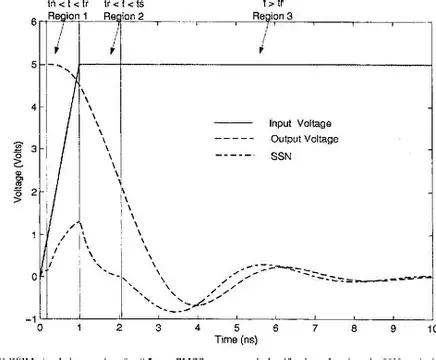
The primary mechanism behind ground bounce is simultaneous switching noise generated by output drivers changing state at the same instant. When many outputs switch from high to low or low to high, the cumulative current surge must flow through the shared ground inductance. Package inductance, via inductance, and the finite impedance of the ground plane itself all contribute to the voltage offset observed at the die. Edge rates below one nanosecond exacerbate the problem because di/dt becomes very large. In addition, split ground planes or poorly placed decoupling networks can force return currents to take longer paths, increasing effective inductance. These factors combine to produce oscillatory ringing on the ground reference that couples into adjacent signal lines.
Effects on Circuit Performance
Ground bounce directly erodes the noise margin of both input and output stages. A positive excursion on ground raises the effective logic-low threshold seen by receiving devices, while a negative excursion can forward-bias protection diodes or cause latch-up in sensitive CMOS structures. Timing skew increases because the actual switching threshold is referenced to a moving ground, leading to setup and hold violations in synchronous designs. Electromagnetic interference also rises as the fluctuating ground acts as an unintended radiator. In extreme cases, cumulative ground bounce across multiple devices can destabilize an entire subsystem, particularly in densely populated boards operating above 100 MHz.
Mitigation Strategies and Best Practices
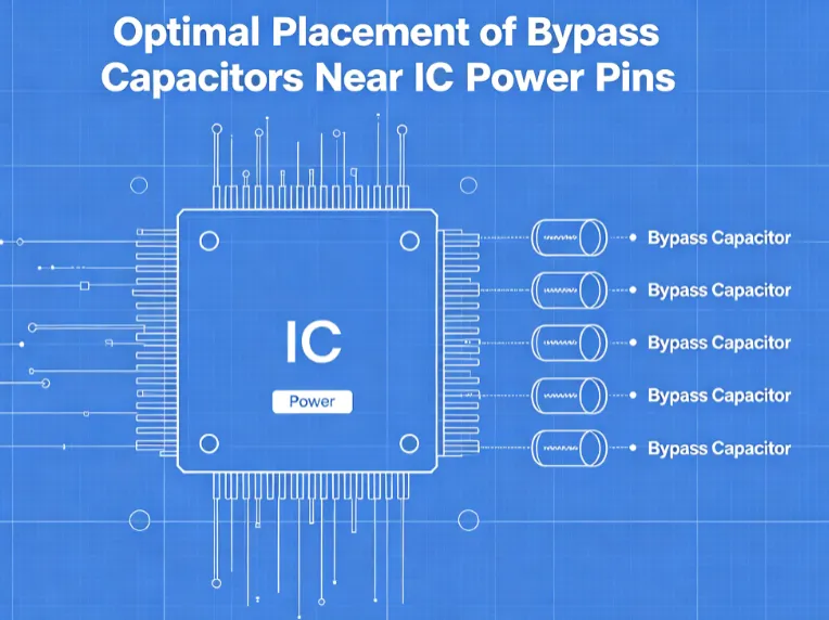
Designers reduce ground bounce by minimizing the inductance of the ground return path. One effective approach is the use of solid, unbroken ground planes on adjacent layers to provide the shortest possible return route for high-speed signals. Strategic placement of decoupling capacitors close to power and ground pins of integrated circuits supplies local charge reservoirs that reduce the current demand on the board-level ground. Via stitching between ground planes further lowers inductance and provides multiple parallel paths. Engineers also control simultaneous switching by staggering output enable timing or grouping outputs that switch together on separate power domains. Adherence to IPC-2221B layout recommendations for return-path continuity and via placement supports these techniques throughout the design process.
Additional measures include selecting packages with lower ground inductance, such as those featuring multiple ground pins or exposed pads, and ensuring that power and ground planes extend fully beneath high-speed devices. Controlled-impedance routing combined with proper termination prevents reflections that would otherwise increase current transients. In boards with mixed analog and digital sections, careful partitioning of ground regions while maintaining a single reference at one point helps isolate sensitive circuits without creating additional inductance.
Conclusion
Ground bounce remains a fundamental consideration in modern PCB design because of ever-increasing clock frequencies and output drive strengths. By addressing return-path inductance through solid planes, strategic decoupling, and layout discipline, engineers can maintain signal integrity and system reliabilhat mitigation measures are integrated from schematic capture through final layout.ity.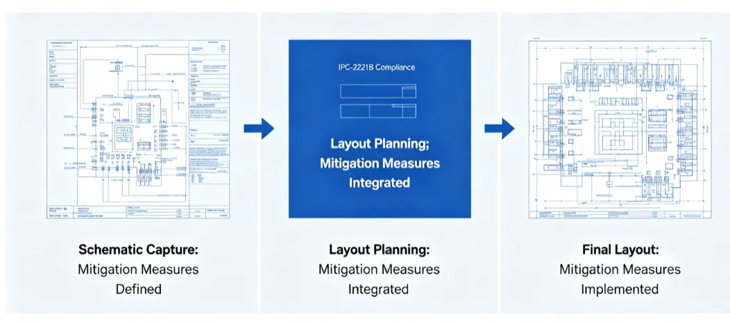
FAQs
Q1: What causes PCB ground bounce in high-speed digital circuits?
A1: Ground bounce arises primarily from rapid current changes during simultaneous switching of multiple outputs, combined with the inherent inductance present in package leads, vias, and ground planes. The resulting voltage fluctuation on the ground reference reduces noise margins and can produce timing errors.
Q2: How does ground bounce affect signal integrity?
A2: Ground bounce shifts the effective reference voltage seen by logic inputs and outputs, leading to false triggering, increased jitter, and potential electromagnetic interference. These effects become more pronounced as edge rates decrease and the number of simultaneously switching outputs increases.
Q3: What layout techniques help mitigate ground bounce?
A3: Techniques include maintaining continuous ground planes, placing decoupling capacitors close to device pins, using multiple ground vias for low-inductance paths, and controlling the number and timing of simultaneous switching outputs. These practices reduce return-path inductance and stabilize the ground reference.
Q4: Are there industry standards that address ground bounce considerations?
A4: Standards such as IPC-2221B provide guidance on printed board design practices that minimize inductance in return paths and support proper power distribution, helping engineers control ground bounce from the initial layout phase.
References
IPC-2221B — Generic Standard on Printed Board Design. IPC, 2012
IPC-6012E — Qualification and Performance Specification for Rigid Printed Boards. IPC, 2017