 ALLPCB


Introduction
Electronic hobbyists embarking on PCB projects with Eagle quickly discover that footprints form the foundation of reliable designs. These footprints define how components sit on the board, influencing everything from soldering to functionality. The Eagle footprint library offers a vast collection of pre-made options, but knowing how to create or modify them unlocks greater flexibility for unique parts. This Eagle PCB tutorial explores the essentials of Eagle component design, helping you streamline your workflow. By mastering Eagle footprint creation, hobbyists can avoid common pitfalls and produce boards that assemble smoothly. Whether prototyping a sensor circuit or a custom controller, proper footprints simplify the entire process.
What Are Eagle PCB Footprints and Why Do They Matter?
Eagle PCB footprints, also known as packages, represent the physical layout of a component on the board. They include copper pads for electrical connections, silkscreen outlines for visual reference, and additional layers for assembly aids. In Eagle component design, a footprint must align precisely with the component's datasheet dimensions to ensure solder joints form correctly. Without accurate footprints, hobbyists face issues like tombstoning in surface-mount parts or poor through-hole connections.
The importance of quality footprints extends to manufacturability and reliability. Standards like IPC-7351B provide guidelines for land pattern dimensions, promoting consistent solder fillet shapes across densities levels. For electronic hobbyists, using the Eagle footprint library prevents trial-and-error during assembly, saving time and materials. Proper Eagle footprint creation also supports automated pick-and-place processes if scaling up from prototypes.
Footprints matter because they bridge schematic symbols and the physical board. Mismatched pads lead to open circuits or shorts, derailing projects. By prioritizing precision in Eagle PCB tutorials, hobbyists build confidence in their designs. Ultimately, well-crafted footprints enable seamless transitions from simulation to fabrication.
Understanding the Layers in Eagle Footprints
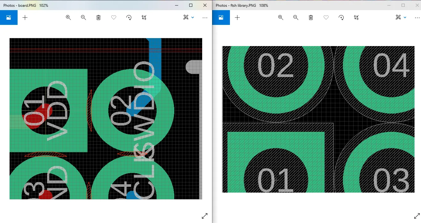
Eagle organizes footprints across multiple layers for comprehensive component representation. Layer 1 handles top-side copper pads, while layer 2 covers bottom-side for double-sided designs. Silkscreen on layers 21 and 22 provides outlines and labels visible after assembly. Name and value texts on layers 25 and 27 help during placement and inspection.
Stop masks on layers 29 and 30 define solder mask openings, preventing bridges between pads. Cream layers 44 and 45 guide stencil application for solder paste in surface-mount assembly. Hobbyists must consider these layers during Eagle component design to match fabrication capabilities. Courtyards on keepout layers ensure spacing between components, reducing interference.
Adhering to structured layers simplifies Eagle footprint library management. Each element serves a purpose, from electrical connectivity to mechanical fit. Understanding these promotes error-free boards. For hobbyists, layering mastery turns complex designs into manageable tasks.
Navigating the Eagle Footprint Library
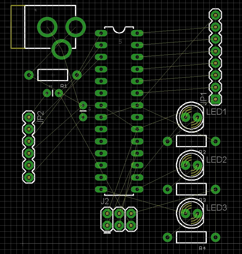
The Eagle footprint library contains thousands of packages for resistors, capacitors, ICs, and connectors, organized by supplier-agnostic categories. Hobbyists access it via the Library Manager, where they can browse, add, or update libraries. Start by searching for standard parts like SOIC or 0805 resistors to populate schematics quickly. Customizing from the library accelerates Eagle component design without starting from scratch.
Libraries update with software versions, incorporating refinements for common components. Verify footprint dimensions against datasheets, as variations exist between manufacturers. The Eagle PCB tutorial approach involves duplicating a similar package and tweaking pads or outlines. This method balances speed and accuracy for hobbyist projects.
Maintaining personal libraries fosters reusability across projects. Export and import options allow sharing with collaborators. Organized libraries reduce design time significantly. For electronic hobbyists, a well-curated Eagle footprint library becomes an invaluable asset.
Step-by-Step Eagle Footprint Creation Guide
Creating a custom footprint in Eagle begins in the Library Manager: select a library, then choose "New Package" and name it descriptively, like RES_0805. Switch to the package editor grid, set to 0.1mm or finer for precision. Place pads using the SMD tool for surface-mount or PIN for through-hole, specifying size, shape, and position from the datasheet. Align pads symmetrically, ensuring pin 1 orientation with a chamfer or dot.
Next, draw silkscreen outlines on layer 21 using the WIRE tool, offsetting 0.1-0.2mm from pads for mask expansion clearance. Add text for name and value on appropriate layers, scaling to 1.0mm height for readability. Define solder mask openings slightly larger than pads to allow proper paste deposition. Include a courtyard rectangle on layer 51 to indicate placement tolerances.
Test the footprint by generating a simple board and running DRC checks for spacing violations. Iterate based on feedback, consulting IPC-7351B for pad geometry recommendations. Save and integrate into a device with a matching symbol. This Eagle footprint creation guide equips hobbyists to handle non-standard parts confidently.
Best Practices for Eagle Component Design
Follow datasheet mechanical drawings religiously, measuring lead pitches and body sizes accurately. Use three density levels from standards: most (LS), nominal (LS), least (XL) for varying fabrication tolerances. Ensure pin 1 indicators are unambiguous to prevent rotation errors during assembly. Maintain consistent naming conventions in the Eagle footprint library, like SOIC_8_3.9X4.9MM.
Optimize pad shapes: rectangular for fine-pitch, oval for gull-wing leads to improve solder flow. Provide adequate silk-to-pad clearance, typically 0.15mm minimum, to avoid mask defects. Incorporate thermal reliefs on through-hole pads for better heat dissipation during soldering. These practices align with J-STD-001 requirements for reliable joints.
Validate footprints with 3D previews if available, or export to STEP for mechanical checks. Document variations in library notes for future reference. Hobbyists benefit from version control in libraries to track changes. Consistent application yields robust designs ready for production.
Common Troubleshooting in Footprint Creation
Hobbyists often encounter tombstoning due to oversized pads causing uneven reflow. Shrink pads per IPC guidelines and balance thermal masses. Misaligned silkscreen leads to placement errors; double-check coordinates against origin. Through-hole holes too tight frustrate hand-soldering; aim for 0.15-0.3mm annular ring.
DRC violations signal courtyard overlaps; expand keepouts as needed. Solder mask bridges arise from inadequate openings; enlarge by pad width plus 0.1mm. Test assemblies with a prototype run to catch issues early. Systematic troubleshooting refines Eagle component design skills over time.
Conclusion
Mastering Eagle PCB footprints transforms hobbyist projects from experimental to professional. The Eagle footprint library provides a solid base, while custom creation handles unique needs. Following this Eagle PCB tutorial and best practices ensures manufacturable boards. Reference standards like IPC-7351B for land patterns to achieve consistency. With practice, simplifying your design process becomes second nature. Start building with confidence today.
FAQs
Q1: What is the Eagle footprint library and how do I access it?
A1: The Eagle footprint library is a collection of pre-defined packages for common components, accessible via the Library Manager in Eagle. Open the manager from the control panel, browse libraries, and add them to your project. Search by name for quick selection during schematic placement. This resource speeds up Eagle component design for hobbyists and helps ensure compatibility with board layouts.
Q2: How does IPC-7351B guide Eagle footprint creation?
A2: IPC-7351B outlines land pattern standards for surface-mount devices, specifying pad sizes and spacings for reliable soldering. In Eagle footprint creation, apply its density levels to match fabrication processes. Measure component leads and calculate toe, heel, and side fillets accordingly. This prevents defects like bridging or insufficient wetting and helps achieve professional results.
Q3: What are common mistakes in Eagle PCB tutorials for footprints?
A3: Beginners often ignore solder mask expansion, leading to bridges, or mismatch pad counts from datasheets. Overlooking pin 1 polarity causes assembly flips. Insufficient courtyard spacing triggers DRC errors. Verify layers and run checks post-creation. Following structured Eagle PCB tutorial steps minimizes these issues for smooth prototyping.
Q4: Can I modify existing footprints in the Eagle footprint library?
A4: Yes. Duplicate a similar package into a personal library, then edit pads, silkscreen, and masks as needed. Reference the component datasheet for accuracy and test in a board file. This approach customizes for variants without altering supplied libraries and supports efficient Eagle component design workflows.
References
SparkFun — Making Custom Footprints in Eagle
IPC-7351B — Generic Requirements for Surface Mount Design and Land Pattern Standard. IPC, 2010
IPC-7251D — Generic Requirements for Through-Hole Design and Land Pattern Standard. IPC, 2011
IPC/JEDEC J-STD-001G — Requirements for Soldered Electrical and Electronic Assemblies. IPC, 2011


