ALLPCB


Introduction
In high-speed PCB designs, electromagnetic interference (EMI) and electromagnetic compatibility (EMC) represent critical challenges that can compromise system reliability. Via-in-pad technology, which places vias directly within component pads, has become essential for achieving the high density required in modern electronics like 5G modules and data centers. This approach shortens signal paths and supports fine-pitch components, but it also influences PCB radiation patterns and overall EMC performance . Engineers must understand how via-in-pad structures interact with electromagnetic fields to optimize via-in-pad EMI mitigation. Improper implementation can lead to impedance discontinuities that radiate unwanted emissions, while proper design enhances signal integrity and reduces susceptibility. This article explores the mechanisms, best practices, and standards guiding via-in-pad EMC in high-speed environments.
What Is Via-in-Pad and Why It Matters for EMI/EMC
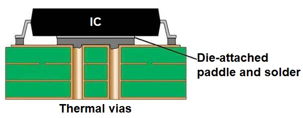
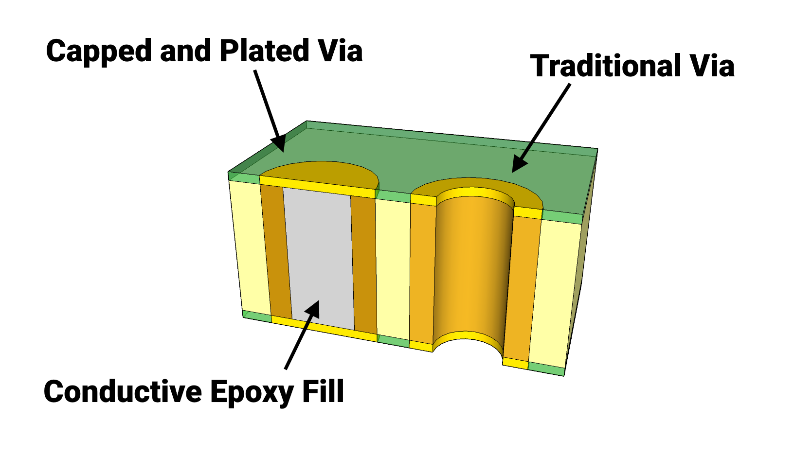
Via-in-pad refers to a PCB interconnect where a via is positioned directly under or within a surface-mount pad, often filled and capped to create a planar surface compatible with component assembly. This technique eliminates the need for additional routing space around the via, enabling denser layouts in high-speed designs. Common in ball grid array (BGA) footprints and high-density interconnect (HDI) boards, it supports signal transitions across layers without extending trace lengths.
The relevance to EMI/EMC stems from the growing frequencies in high-speed design EMI scenarios, where signals exceed 1 GHz. Standard dogbone vias increase loop areas for return currents, promoting PCB radiation and via-in-pad EMI. In contrast, via-in-pad reduces these loops, lowering inductance and potential emission sources. Compliance with standards like IPC-4761 ensures reliable via protection, directly impacting EMC design outcomes. For electric engineers, mastering this balance prevents failures in radiated emissions testing.
Via-in-pad also addresses thermal and mechanical demands in dense boards, but its electromagnetic effects demand careful consideration during layout.
Technical Principles of Via-in-Pad on EMI/EMC
Vias inherently introduce parasitic inductance and capacitance, acting as stubs that resonate at quarter-wavelength frequencies, converting guided signals into radiated fields. In via-in-pad configurations, the via's proximity to the pad alters impedance transitions, potentially causing reflections if mismatched to the 50-ohm trace characteristic impedance. These discontinuities amplify high-speed design EMI, especially above 2 GHz, where even small inductances of 1-2 nH distort eye diagrams and increase crosstalk .
Filled via-in-pad, as defined in IPC-6012 for Class 3 boards, mitigates this by eliminating air voids and solder wicking risks. The conductive or non-conductive fill provides a uniform dielectric interface, reducing parasitic effects and via-in-pad EMC vulnerabilities. Capping with copper further planarizes the surface, minimizing surface wave propagation that contributes to PCB radiation. Ground return paths through adjacent stitching vias create shielding cages, confining fields and lowering emissions.
At higher frequencies, unfilled vias behave inductively, elevating impedance by factors of 3-4 times, while optimized via-in-pad maintains flatter profiles up to 40 GHz with proper antipad sizing [3]. Loop inductance, proportional to via length and diameter, drops significantly with microvias spanning fewer layers. This principle underpins EMC design, where return current proximity via ground planes suppresses differential-mode radiation.
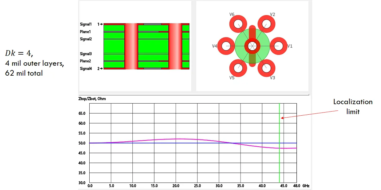
Electromagnetic coupling between vias exacerbates EMI if spacing falls below wavelength/20 guidelines. In multilayer stackups, via-in-pad placed near solid ground planes leverages image currents for cancellation, enhancing overall immunity.
Mechanisms Causing EMI in Via-in-Pad Designs
Impedance mismatches at via transitions generate voltage standing waves, leading to power leakage as radiated EMI. For instance, abrupt pad-to-via geometry changes exceed 10% deviation from nominal impedance, reflecting energy backward and forward. In high-speed paths, multiple vias compound this, creating comb-like filters that peak at harmonics, intensifying PCB radiation.
Stub effects from through-vias extend beyond the signal layers, resonating and radiating like antennas. Via-in-pad counters this by using blind or buried variants, shortening stubs and confining fields. However, without filling, voids trap contaminants or create uneven fills, distorting fields and inviting via-in-pad EMI.
Crosstalk arises from mutual inductance between adjacent vias, particularly in arrays under BGAs. Poor ground referencing allows common-impedance coupling, where shared return paths modulate signals. Radiation from clock edges couples through these paths, failing EMC limits.
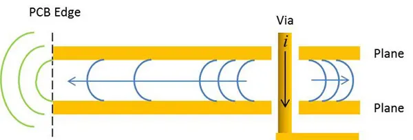
Susceptibility follows reciprocity: structures radiating easily also pick up interference. Dense via-in-pad fields interact with external sources, inducing noise in sensitive nets.
Practical Solutions and Best Practices for Via-in-Pad EMI Reduction
To optimize via-in-pad EMC, select fill materials per IPC-4761 Type VII specifications, ensuring dimples below 76 microns for Class 3 and uniform coverage. Non-conductive epoxy suffices for signals, while conductive fills aid power or thermal paths without shorting risks. Always cap vias to prevent solder flow during reflow.
Incorporate ground stitching vias at a 1:1 ratio around signal via-in-pad, spaced at 8-12 mils to form via fences. This provides low-inductance returns, reducing loop areas by up to 50% and shielding RF sections [1]. Position antipads to tune capacitance, targeting 50-ohm via impedance via field solvers.
Minimize via count in critical nets, favoring microvias (0.2 mm diameter) over through-holes to cut inductance. Route high-speed traces on inner layers adjacent to ground planes, avoiding splits. Back-drill longer vias to remove stubs in 10 Gbps+ designs.
For stackups, dedicate layers to ground near signals, using via-in-pad for transitions. Simulate S-parameters to verify return loss below -20 dB.
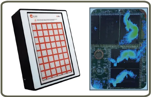
Fabrication tolerances demand 2-mil annular rings externally per IPC-6012 Class 3, with 6-mil clearance from adjacent features. Test prototypes with near-field probes to map emissions.
Troubleshooting Common Via-in-Pad EMI Issues
Engineers often encounter elevated emissions from BGA fanouts lacking stitching. Solution: Add perimeter ground vias, verifying spacing maintains lambda/20 at peak frequencies. Simulate pre-layout to predict hotspots.
Solder voids post-assembly indicate inadequate filling; X-ray inspect and iterate fill processes. Reflections show as eye closure; adjust pad geometry iteratively.
Thermal stress warps boards, cracking fills and opening EMI paths. Use symmetric stackups and thermal vias.
Conclusion
Via-in-pad profoundly shapes EMI/EMC in high-speed PCBs by enabling density while demanding precise control over parasitics and returns. Filled and stitched implementations per IPC standards minimize PCB radiation and enhance robustness. Electric engineers benefit from shorter paths and lower inductance, but must prioritize impedance matching and shielding. Adopting these practices ensures compliance and performance in demanding applications.
FAQs
Q1: What is via-in-pad EMI and how does it affect high-speed designs?
A1: Via-in-pad EMI arises from parasitic effects in vias placed within pads, causing impedance mismatches and radiation in high-speed signals above 1 GHz. Shorter paths reduce loop inductance, but unfilled voids or poor grounding amplify emissions. Best practices include epoxy filling and stitching vias to maintain EMC design integrity, preventing failures in radiated tests .
Q2: How does via-in-pad improve EMC performance compared to standard vias?
A2: Via-in-pad shortens stubs and integrates seamlessly with pads, lowering inductance by up to 50% and reflections below 0.1 coefficient. This confines fields better than dogbone styles, reducing PCB radiation susceptibility. Standards like IPC-4761 Type VII ensure uniform fills, vital for via-in-pad EMC in dense layouts.
Q3: What are key best practices for via-in-pad in high-speed design EMI mitigation?
A3: Use microvias with 0.2 mm diameters, 1:1 ground stitching, and antipad tuning for 50-ohm matches. Fill and cap per IPC-6012 Class 3 to avoid voids. Route near unbroken ground planes and simulate for low return loss.
Q4: Can via-in-pad structures cause increased EMI if not designed properly?
A4: Yes, mismatches over 10% or extended stubs resonate, radiating harmonics and increasing via-in-pad EMI. Inadequate shielding leads to crosstalk and poor returns. Proper filling, spacing, and stackup planning per IPC guidelines counteract these risks effectively.
References
IPC-4761 — Design Guide for Protection of Vias. IPC
IPC-6012E — Qualification and Performance Specification for Rigid Printed Boards. IPC
IPC-2221B — Generic Standard on Printed Board Design. IPC