 ALLPCB


Step-up stencils provide a single-tool approach to solder paste deposition across boards that require different paste volumes. Engineers often face boards with both fine-pitch components and larger pads, and a step-up stencil allows controlled paste release in one printing pass. This design reduces the need to switch between multiple stencils during production runs. Procurement teams evaluate step-up stencil cost against the expense of ordering and managing separate stencils for each thickness requirement. The decision ultimately rests on production volume, changeover time, and long-term yield improvements.
What Is a Step-Up Stencil and Why It Matters
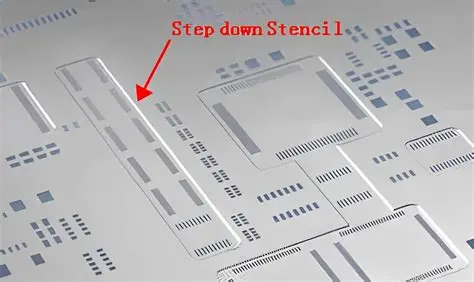
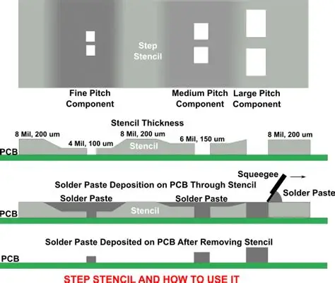
A step-up stencil features localized thickness increases in selected areas while maintaining a thinner base elsewhere. The thicker sections deliver higher paste volumes to larger pads or through-hole components, whereas the thinner base supports fine-pitch devices. This construction directly addresses the challenge of achieving consistent solder joints without over- or under-depositing paste. In high-mix assembly environments, the approach minimizes stencil changes and associated downtime. Engineers therefore examine step-up stencil price alongside the cumulative costs of multiple stencils, storage, and repeated setup procedures.
Industry standards such as IPC-A-610 guide acceptable solder joint criteria that influence stencil thickness choices. When boards contain mixed component types, a single step-up stencil can satisfy volume requirements for both categories in one operation. This capability becomes especially relevant for contract manufacturers handling frequent product variants. The resulting reduction in handling steps contributes to overall process stability and lower defect rates.
Technical Principles of Step-Up Stencil Construction
Step-up stencils are typically fabricated from stainless steel sheets that receive selective material addition or etching to create raised zones. The transition between thin and thick regions must maintain smooth edges to prevent paste scooping or incomplete release. Proper design accounts for the aspect ratio and area ratio rules that govern paste transfer efficiency. Engineers calculate the required step height based on target paste volume for each pad geometry. These calculations rely on established formulas rather than trial-and-error adjustments during production.
The mechanical integrity of the step remains critical because repeated squeegee passes can cause deformation if the step is not adequately supported. Finite-element analysis during design helps predict stress distribution and ensure the stencil retains flatness over its service life. In practice, the step-up configuration delivers consistent paste deposits across the board without requiring separate printing operations. This consistency directly supports higher first-pass yields and reduces rework associated with insufficient or excessive solder.
Related Reading: When and Why to Use a Step Up Stencil in Your PCB Project
Practical Comparison of Step-Up Stencil Cost Versus Multiple Stencils
When comparing step-up stencil cost to the price of ordering several individual stencils, the initial investment in a step-up design often appears higher. However, the total cost of ownership includes factors such as setup time, storage space, and the risk of using the wrong stencil during changeovers. Multiple stencils require additional handling, cleaning cycles, and verification steps that accumulate over hundreds of production lots. A step-up stencil eliminates these repeated operations, translating into measurable labor savings and reduced machine idle time.
ROI calculations typically factor in reduced changeover minutes per shift and the avoidance of paste-volume-related defects. For medium to high production volumes, the payback period frequently falls within the first few months of use. Lower-volume or highly variable boards may still favor multiple stencils if the step-up design cannot accommodate extreme thickness differences. Engineers therefore review board complexity and annual run rates before finalizing the stencil strategy.
Best Practices for Justifying Step-Up Stencil Investment
Begin the justification process by documenting current defect rates traceable to paste volume mismatch. Next, obtain quotes for both a step-up stencil and the equivalent set of separate stencils, then calculate total cost per board produced. Include the value of improved throughput and lower scrap rates in the model. Validate the design through a small pilot run that measures actual paste volume and joint quality against IPC-A-610 acceptance criteria. This data-driven approach provides clear evidence for procurement decisions.
Ongoing monitoring of stencil wear and print quality further supports the cost-justification case. Regular inspection reveals whether the step-up features maintain performance over the expected stencil life. When these practices are followed, the step-up stencil cost justification becomes straightforward and defensible to management.
Troubleshooting Insights for Step-Up Stencil Performance
Common issues with step-up stencils include paste bridging at step transitions or incomplete release in the thinner zones. These problems usually trace back to insufficient step-edge radius or incorrect squeegee pressure settings. Adjusting print parameters while keeping the stencil design fixed often resolves the symptoms without additional tooling expense. When defects persist, engineers review the area ratio at each pad location to confirm the step height matches the required paste volume.
Documentation of print results across multiple lots helps identify whether the issue stems from the stencil itself or from upstream process variables. Consistent application of these troubleshooting steps maintains the expected ROI by avoiding unplanned downtime.
Related Reading: Mastering Step Up Stencils: A Comprehensive Guide for PCB Assembly
Conclusion
Step-up stencils offer a practical route to balancing paste volume requirements on complex boards while controlling overall process costs. By comparing step-up stencil price against the cumulative expense of multiple stencils, engineers can identify clear opportunities for improved efficiency and yield. Structured evaluation using established industry standards ensures decisions rest on measurable data rather than assumptions. When properly designed and maintained, the approach delivers sustained value across a range of production scenarios.
FAQs
Q1: How does step-up stencil cost compare to ordering multiple stencils for the same board?
A1: A step-up stencil typically carries a higher initial price than any single conventional stencil, yet the total expenditure often proves lower when changeover labor, storage, and defect-related rework are included. Production teams calculate the break-even point by tracking minutes saved per setup and the reduction in solder-related defects. For boards with moderate to high annual volumes, the step-up stencil cost justification becomes evident within the first production quarter.
Q2: What factors determine whether step-up stencil ROI justifies the investment?
A2: ROI depends on board complexity, annual production quantity, and the frequency of stencil changes required by the current process. Engineers review paste-volume mismatch defects and machine idle time to quantify savings. When these metrics show meaningful improvement, the step-up stencil ROI typically supports the decision over continued use of multiple stencils.
Q3: Can a step-up stencil replace multiple stencils without compromising print quality?
A3: Properly designed step-up stencils maintain or improve print quality by delivering the correct paste volume to each pad type in a single pass. Quality remains consistent when area-ratio guidelines are followed and step transitions are engineered for smooth paste release. Validation runs confirm that defect rates stay within acceptable limits defined by industry standards.
Q4: How do engineers calculate step-up stencil cost justification for a new project?
A4: Engineers compile quotes for both options, then add the projected costs of setup time, cleaning cycles, and potential rework. They compare these totals against expected yield gains and throughput increases. The resulting cost-per-board figure provides the quantitative basis for approving the step-up stencil investment.
References
IPC-A-610G — Acceptability of Electronic Assemblies. IPC, 2017
J-STD-005A — Requirements for Soldering Pastes. IPC, 2016


