In the fast-paced world of PCB (Printed Circuit Board) design and assembly, precision is everything. If you're working on a project with complex components like Ball Grid Arrays (BGA), Quad Flat No-lead (QFN) packages, or mixed technology boards, you might have come across the term "step-up stencil." So, when should you use a step-up stencil, and why is it beneficial? Simply put, a step-up stencil is ideal for projects requiring different solder paste volumes for various components on the same board, such as BGAs and QFNs in mixed technology designs. It helps ensure precise solder application, reduces defects, and improves assembly quality.
In this blog, we'll dive deep into the specifics of step-up stencil applications, explore their advantages, and explain how they cater to unique challenges in PCB projects. Whether you're an engineer or a designer looking to optimize your assembly process, this guide will provide actionable insights to help you make informed decisions.
What Is a Step-Up Stencil and How Does It Work?
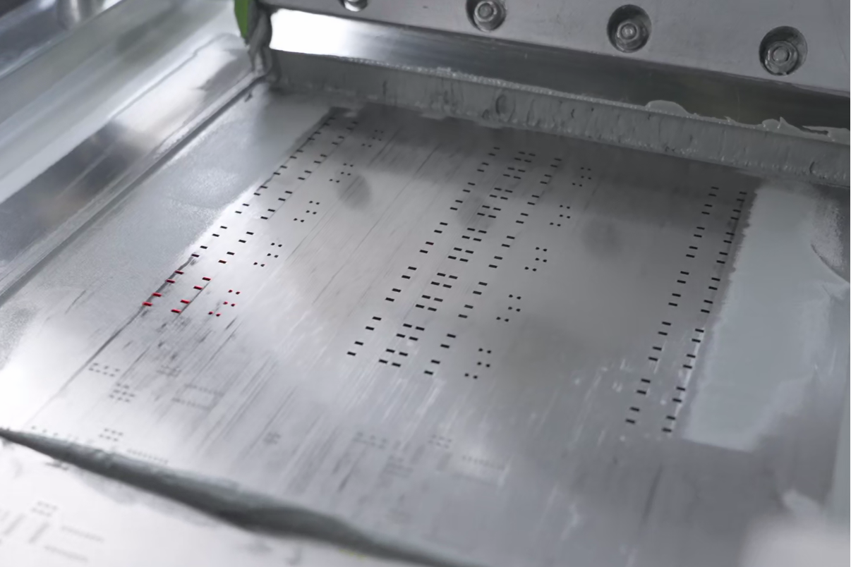
A step-up stencil is a specialized tool used in the surface mount technology (SMT) assembly process to apply solder paste onto a PCB. Unlike a standard stencil, which has a uniform thickness, a step-up stencil features areas of varying thickness. These "steps" allow for different amounts of solder paste to be deposited on different parts of the board during a single printing process.
For instance, components like BGAs often require more solder paste due to their numerous, closely spaced connections, while smaller components like QFNs might need less to avoid issues like bridging or insufficient solder joints. The thicker areas of a step-up stencil cater to high-volume solder needs, while thinner areas ensure precision for smaller pads.
The stencil is typically made from stainless steel and is laser-cut to match the PCB layout. During the assembly process, it is placed over the board, and solder paste is spread across it using a squeegee. The varying thicknesses control the paste volume, ensuring each component gets the right amount for a reliable connection.
Key Applications of Step-Up Stencils in PCB Projects
Step-up stencils are not a one-size-fits-all solution, but they shine in specific scenarios. Below are the primary step-up stencil applications where they deliver significant value.
1. Mixed Technology Boards
Mixed technology boards combine different types of components, such as through-hole, surface-mount, and fine-pitch devices, on a single PCB. These boards often have varying solder paste requirements. For example, a larger connector might need a thicker deposit of solder paste (around 0.15mm) to ensure a strong joint, while a tiny 0402 resistor might only require a thinner layer (about 0.1mm) to prevent excess paste and potential shorts.
A step-up stencil addresses this by allowing multiple paste volumes in one print cycle, streamlining the assembly process and reducing the need for multiple stencils or manual adjustments. This is particularly useful in step-up stencil for mixed technology projects, where efficiency and accuracy are critical.
2. BGA Components
Ball Grid Arrays (BGAs) are widely used in modern electronics due to their high pin density and compact size. However, their assembly can be challenging because the solder balls underneath require a consistent and adequate volume of paste—often more than other components on the board. Insufficient paste can lead to weak joints, while excess paste risks bridging between connections.
Using a step-up stencil for BGA components allows designers to increase the stencil thickness (e.g., to 0.2mm) over BGA pads, ensuring the right amount of solder paste is applied. This precision minimizes defects and enhances the reliability of connections, especially in high-density designs.
3. QFN Packages
Quad Flat No-lead (QFN) packages are popular for their small footprint and excellent thermal performance, often used in power management and RF applications. Unlike BGAs, QFNs have exposed pads on the bottom for heat dissipation and grounding, requiring careful control of solder paste to avoid voids or insufficient coverage.
A step-up stencil for QFN can be tailored to provide just the right amount of paste for these pads—often a thinner layer (around 0.08mm to 0.1mm) compared to BGAs. This helps achieve optimal thermal and electrical performance while preventing issues like floating components during reflow soldering.
Advantages of Using Step-Up Stencils in PCB Assembly
Now that we've covered the applications, let's explore the step-up stencil advantages that make them a valuable choice for specific PCB projects. These benefits directly impact assembly quality, cost-efficiency, and production timelines.
1. Precision in Solder Paste Application
One of the standout benefits of step-up stencils is their ability to deposit precise amounts of solder paste tailored to each component's needs. For instance, a typical BGA might require a paste volume of 0.0012 cubic millimeters per pad, while a QFN thermal pad might need only 0.0008 cubic millimeters to avoid excess. A step-up stencil ensures these variations are managed in a single pass, reducing the risk of defects like open circuits or solder bridges.
2. Reduced Assembly Defects
Defects in SMT assembly, such as tombstoning, insufficient solder, or bridging, can lead to costly rework or product failures. Step-up stencils minimize these issues by customizing paste volume to component requirements. Studies in SMT processes suggest that using variable-thickness stencils can reduce defect rates by up to 20% in mixed technology boards, saving time and resources during production.
3. Cost and Time Efficiency
Without a step-up stencil, manufacturers might need multiple stencils or additional printing steps to accommodate different solder paste volumes. This increases both material costs and production time. A single step-up stencil eliminates these extra steps, streamlining the process. For high-volume production runs, this can translate to significant savings—sometimes reducing stencil-related costs by 15-30% per batch.
4. Enhanced Reliability for Complex Designs
As PCB designs grow more complex with tighter tolerances and smaller components, reliability becomes paramount. Step-up stencils support consistent solder joint formation, which is critical for long-term performance in applications like automotive electronics or medical devices. For example, in a BGA with a 0.4mm pitch, even a slight deviation in solder volume can cause failures under thermal stress. A step-up stencil helps maintain uniformity, ensuring the board withstands operational demands.
5. Flexibility for Diverse Component Types
The ability to handle multiple component types on the same board is a game-changer. Whether you're working on a board with a mix of BGAs, QFNs, and traditional SMT components, a step-up stencil adapts to the diverse needs without compromising quality. This flexibility is a key reason why step-up stencils are often preferred in step-up stencil for mixed technology projects.
When Should You Use a Step-Up Stencil?
While step-up stencils offer clear benefits, they aren't necessary for every PCB project. Here are the key scenarios where they are most effective:
- High-Density Designs: If your board includes fine-pitch components like BGAs with a pitch of 0.5mm or less, a step-up stencil ensures accurate solder paste volume.
- Mixed Component Sizes: When your design combines large connectors or power components with tiny passives, varying stencil thickness prevents over- or under-pasting.
- Critical Reliability Needs: For applications where failure is not an option—think aerospace or medical devices—step-up stencils reduce assembly risks.
- Volume Production: In large-scale manufacturing, the efficiency of a single stencil with multiple thicknesses outweighs the initial design cost.
On the other hand, for simpler boards with uniform component types and solder requirements, a standard stencil might suffice. The decision often comes down to balancing cost with the complexity of your design.
Challenges and Considerations with Step-Up Stencils
While the advantages are compelling, it's important to be aware of potential challenges when using step-up stencils. Addressing these upfront can help you avoid pitfalls during assembly.
1. Higher Initial Cost
Designing and manufacturing a step-up stencil is more complex than a standard one, leading to higher upfront costs. The process often involves advanced laser etching to create precise steps, which can add 10-20% to the stencil price. However, this cost is often offset by reduced defects and faster production in larger runs.
2. Design Complexity
Creating a step-up stencil requires detailed collaboration between the PCB designer and the stencil manufacturer. You’ll need to specify exact thicknesses for different areas (e.g., 0.15mm for BGAs and 0.1mm for QFNs), which adds a layer of complexity to the design phase. Errors in specification can lead to improper solder deposits, so accuracy is critical.
3. Limited Applicability
Step-up stencils are specialized tools best suited for specific scenarios. If your project doesn’t involve varying solder paste needs, investing in one might not be justified. Evaluate your board’s requirements before opting for this solution.
Best Practices for Implementing Step-Up Stencils
To maximize the benefits of step-up stencils in your PCB project, follow these practical tips:
- Collaborate Early: Work closely with your stencil provider during the design phase to ensure the step thicknesses match your component needs. Provide detailed Gerber files and component datasheets for accuracy.
- Test Before Full Production: Run a small batch with the step-up stencil to verify solder paste distribution. Use X-ray inspection to check for voids or bridging, especially under BGAs and QFNs.
- Optimize Reflow Profiles: Adjust your reflow oven settings to account for varying solder volumes. For instance, a BGA area with more paste might need a slightly longer soak time to ensure even melting.
- Maintain Stencil Cleanliness: Solder paste residue can accumulate in the stepped areas, affecting print quality. Regular cleaning with appropriate solvents ensures consistent performance.
Conclusion: Elevating Your PCB Assembly with Step-Up Stencils
Step-up stencils are a powerful tool for tackling the challenges of modern PCB assembly, especially in projects involving BGAs, QFNs, and mixed technology designs. Their ability to deliver precise solder paste volumes tailored to each component’s needs makes them invaluable for reducing defects, improving reliability, and streamlining production. Whether you're optimizing a step-up stencil for BGA connections or leveraging step-up stencil advantages in a complex mixed technology board, this solution can elevate the quality of your final product.
By understanding the specific step-up stencil applications and weighing the benefits against the challenges, you can make an informed decision about when to integrate this technology into your workflow. For engineers and designers aiming for precision and efficiency, a step-up stencil could be the key to unlocking superior assembly results in your next PCB project.
 ALLPCB


