 ALLPCB


Introduction
Rigid printed circuit board (PCB) assembly forms the backbone of most electronic devices, from consumer gadgets to industrial controls. As supply chain disruptions and raw material fluctuations drive up costs, electrical engineers face pressure to optimize manufacturing without sacrificing performance or reliability. Effective PCB assembly cost reduction requires a multifaceted approach, targeting design, materials, and processes. This article outlines practical strategies such as component sourcing strategies, optimizing PCB panelization, reducing PCB layer count, and alternative materials for PCB. These methods help balance budget constraints with adherence to quality benchmarks like IPC-6012F for rigid board specifications. Engineers can implement these tactics early in the design phase to yield substantial savings across production runs.
High-volume production amplifies the need for cost control, as even minor inefficiencies scale dramatically. Engineers must evaluate trade-offs between functionality and economy, ensuring designs meet performance needs without over-specification. Troubleshooting common issues like warpage or solder joint failures early prevents costly rework. Standards such as J-STD-001J provide guidelines for soldering processes that minimize defects and associated expenses. By dissecting these elements, teams can shift from reactive fixes to proactive optimization.
Understanding Rigid Board Assembly and Key Cost Drivers
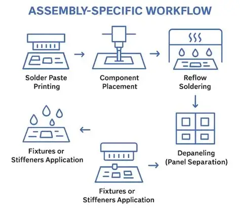
Rigid PCB assembly encompasses soldering surface-mount and through-hole components onto non-flexible boards, typically using automated pick-and-place machines, reflow ovens, and inspection tools. Costs arise primarily from materials, labor, equipment setup, and yield losses due to defects. For instance, multilayer boards demand more lamination cycles and drilling operations, inflating expenses exponentially. Component procurement often accounts for 40 to 60 percent of total assembly costs, depending on part complexity and availability. Panelization inefficiencies lead to material waste, while excessive layer counts increase fabrication time and handling risks. Recognizing these drivers empowers engineers to prioritize high-impact interventions for PCB assembly cost reduction.
High-volume production amplifies the need for cost control, as even minor inefficiencies scale dramatically. Engineers must evaluate trade-offs between functionality and economy, ensuring designs meet performance needs without over-specification. Troubleshooting common issues like warpage or solder joint failures early prevents costly rework. Standards such as J-STD-001J provide guidelines for soldering processes that minimize defects and associated expenses. By dissecting these elements, teams can shift from reactive fixes to proactive optimization.
Technical Principles Behind Assembly Costs
The core mechanisms driving rigid PCB assembly costs stem from material properties, layout density, and processing tolerances. Base materials like epoxy laminates dictate thermal expansion coefficients, influencing warpage during reflow and requiring precise control to avoid defects. Thicker copper foils enhance current capacity but raise etching costs and increase impedance mismatches in high-speed signals. Layer count directly correlates with via drilling, plating, and registration accuracy, where misalignment in multilayers demands advanced alignment systems. Component density affects stencil design and paste volume, with fine-pitch parts risking bridging or insufficient solder. Optimizing these parameters reduces cycle times and scrap rates, fundamental to PCB assembly cost reduction.
Panelization leverages economies of scale by grouping multiple boards on a single substrate, but poor nesting leads to edge effects and depanelization waste. Vias and blind/buried structures add sequential buildup steps, escalating fabrication complexity. Solder mask and silkscreen layers, while essential for protection, incur additional printing and curing operations if not standardized. Electrical engineers must model these interactions using stackup calculators to predict cost implications accurately. Adherence to IPC-A-610J criteria during inspection ensures only viable assemblies proceed, curbing downstream failures.
Material alternatives alter dielectric constants and mechanical strength, impacting signal integrity and manufacturability. For example, thinner cores reduce weight and material usage but necessitate tighter tolerances in lamination. Thermal management features like embedded planes add value yet complicate routing. Understanding these principles guides engineers toward designs that streamline assembly flows.
Practical Strategies for Cost Reduction
Component Sourcing Strategies
Selecting components is pivotal for PCB assembly cost reduction, as exotic or obsolete parts inflate lead times and pricing. Prioritize standard footprints like 0805 or QFN packages, which benefit from high supplier volumes and automated handling compatibility. Bulk purchasing from multiple vetted distributors mitigates shortages while negotiating volume discounts. Engineers should perform obsolescence checks during schematic capture, opting for long-lifecycle alternatives without performance trade-offs. Dual-sourcing critical passives ensures continuity, avoiding single-point failures in supply chains. These component sourcing strategies can cut material costs by streamlining procurement and reducing change orders.
Avoid custom leads or polarities that demand manual intervention, favoring reel-packed parts for uninterrupted SMT lines. Value analysis on resistors and capacitors reveals opportunities to upsize for tolerance without added expense. Integrating these practices early prevents redesign loops that erode budgets.
Optimizing PCB Panelization
Optimizing PCB panelization maximizes substrate utilization, directly targeting material waste in rigid board production. Standardize array dimensions to match fabricator panels, typically 18x24 inches, using V-scoring or tab routing for efficient depaneling. Nest irregular shapes tightly with rotation algorithms to exceed 80 percent utilization, minimizing kerf losses. Fiducials and breakaway tabs facilitate precise alignment during assembly, reducing setup errors. Engineers should simulate panels in layout software, balancing yield against rail widths for handling stability. This approach slashes per-board material costs significantly.
Consider assembly flow: orient components away from score lines to prevent stress cracks during separation. Multi-up panels enable parallel processing in reflow, shortening throughput times. Troubleshooting panel warpage involves symmetric layouts and balanced copper distribution.
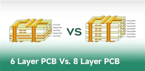
Reducing PCB Layer Count
Reducing PCB layer count streamlines fabrication by eliminating inner layer imaging and lamination presses. Consolidate signals using microvias or embedded components where feasible, adhering to via current ratings per IPC-6012F. Ground and power planes serve dual purposes, freeing signal layers for routing. Engineers can employ differential pairs and controlled impedance to maintain integrity on fewer layers. For four-layer boards, optimize stackups with signal-ground-signal-ground configurations to suppress noise without extras. This strategy cuts drilling and plating steps, yielding faster turnaround and lower expenses.
Evaluate signal speed requirements; many mid-range designs suffice with two or four layers. Troubleshooting crosstalk involves stitching vias rather than full planes. Layer minimization demands iterative simulation but pays dividends in cost savings.
Alternative Materials for PCB
Alternative materials for PCB offer cost-effective substitutes for demanding applications without compromising basics. Standard FR-4 suits most rigid boards, but composite epoxy materials provide viable options for low-frequency, single/double-layer designs. These alternatives reduce resin content and improve machinability, lowering tooling costs. High glass transition temperature variants add expense only when thermal cycling exceeds 130 degrees Celsius. Engineers should match CTE to components per J-STD-001J to avoid solder joint stress. Selecting based on electrical and mechanical needs optimizes budgets.
Thinner copper weights like 1 oz/ft2 suffice for low-power circuits, easing etching and reducing chemical usage. Paper-phenolic composites work for non-critical prototypes, though limited by moisture absorption. Practical testing validates choices through thermal shock simulations.
Related Reading: SMT vs. Through Hole: A Cost Analysis Showdown for PCB Assembly
Troubleshooting Common Cost Overruns
Engineers often encounter cost overruns from poor DFM, such as excessive vias causing drill breakage or non-standard drill sizes inflating setups. Panel yield drops if copper imbalance induces bow, addressed by symmetric pours and bake-out processes. Component misalignment in high-density areas stems from stencil misalignment; verify aperture ratios at 1:1 land-to-aperture. Solder defects per IPC-A-610J, like insufficient fillet, arise from paste viscosity issues, resolved by viscosity checks. Layer registration failures in multilayers demand sequential lamination controls. Proactive DFM reviews and pilot runs pinpoint these, enabling targeted PCB assembly cost reduction.
Related Reading: The Hidden Cost of Warped PCBs: How to Avoid Assembly Failures
Conclusion
Achieving cost-effective rigid board assembly hinges on integrated strategies across design, sourcing, and processing. Component sourcing strategies secure affordable, reliable parts; optimizing PCB panelization curbs waste; reducing PCB layer count simplifies fabrication; and alternative materials for PCB tailor expenses to needs. Electrical engineers benefit from early collaboration with manufacturers, leveraging standards like IPC-6012F, J-STD-001J, and IPC-A-610J for quality assurance. These practices not only lower costs but enhance yield and reliability. Implementing them positions teams for competitive advantage in volume production.
FAQs
Q1: What are effective component sourcing strategies for PCB assembly cost reduction?
A1: Focus on standard package sizes and footprints to leverage bulk pricing and automation compatibility. Dual-source critical components to avoid shortages and negotiate volume discounts with distributors. Perform early obsolescence analysis to select long-lifecycle parts, minimizing redesign costs. These steps ensure reliable supply chains while cutting material expenses significantly.
Q2: How does optimizing PCB panelization contribute to manufacturing savings?
A2: Panelization maximizes substrate use by nesting multiple boards efficiently on standard arrays, reducing material waste. Use V-scoring or tabs for clean depaneling and place fiducials for alignment. Simulate layouts to achieve over 80 percent utilization, shortening setup and processing times. This directly lowers per-unit costs in rigid assembly.
Q3: Can reducing PCB layer count maintain performance while lowering costs?
A3: Yes, by optimizing routing with planes and microvias per IPC-6012F guidelines. Fewer layers cut lamination and drilling steps, ideal for mid-speed signals. Balance copper for symmetry to prevent warpage. Simulations verify integrity, ensuring cost savings without functionality loss.
Q4: What alternative materials for PCB offer cost benefits in rigid designs?
A4: Composite epoxies like CEM series suit simple boards, reducing resin and machining costs versus high-Tg FR-4. Match CTE to components per J-STD-001J for joint reliability. Thinner foils ease etching for low-power apps. Test for your application's thermal and electrical needs.


