ALLPCB


Introduction
In the world of electronic hobbyists, creating a personal lab space goes beyond just tools and components. It involves thoughtful choices that align with sustainable electronics practices, reducing environmental impact while ensuring safety. The halogen-free approach stands out as a practical way to build an eco-friendly electronics lab, focusing on materials that minimize toxic emissions during manufacturing, assembly, and even potential fires. Halogens like chlorine and bromine, common in traditional flame retardants, release harmful gases when burned, posing risks in home workshops. By adopting halogen-free alternatives, hobbyists can craft a halogen-free workbench that supports environmental electronics without compromising performance. This guide explores how to set up such a lab step by step, drawing on factory-level insights for reliable results.
What Is a Halogen-Free Approach and Why It Matters for Hobby Labs
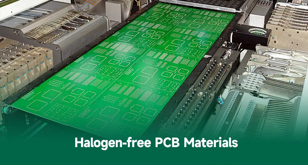
A halogen-free electronics setup eliminates halogens from PCBs, solders, fluxes, and components, typically limiting chlorine and bromine to under 900 parts per million each and total halogens below 1500 parts per million. This definition aligns with established industry benchmarks, ensuring materials meet rigorous purity levels. For electronic hobbyists, this matters because home labs often involve soldering irons, heat guns, and storage in confined spaces where fire safety is critical. Traditional halogenated materials can produce corrosive and toxic smoke, affecting health and nearby electronics. In contrast, a sustainable electronics lab using halogen-free materials promotes cleaner air, easier recycling, and compliance with global trends toward environmental electronics. Hobbyists benefit from reduced long-term hazards, making projects safer for repeated use.
The relevance extends to the growing demand for eco-conscious practices among makers and tinkerers. As hobby labs evolve into semi-professional spaces, selecting halogen-free options future-proofs investments against stricter regulations. These materials often feature enhanced thermal stability, resisting delamination under heat cycles common in prototyping. Factory-driven standards guide this shift, emphasizing verifiable material specs over untested substitutes. Ultimately, an eco-friendly electronics lab not only lowers ecological footprints but also builds confidence in project durability.
Technical Principles Behind Halogen-Free Materials
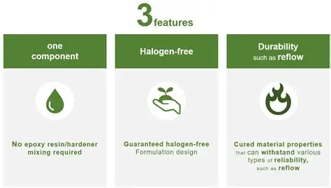
Halogen-free PCBs replace traditional brominated flame retardants with phosphorus or nitrogen-based compounds embedded in epoxy resins. These alternatives interrupt combustion at the molecular level by forming char layers that block oxygen, achieving similar fire resistance without halogens. IPC-4101E outlines specifications for such base materials, covering rigid and multilayer boards with precise qualification tests for flame retardancy. The result is materials with higher glass transition temperatures, often suited for lead-free soldering processes that demand elevated reflow profiles. In a hobby lab context, this means boards withstand repeated rework without warping or degrading insulation.
Decomposition temperatures also improve, reducing risks during high-heat operations like desoldering components. Nitrogen-phosphorus synergies enhance insulation resistance post-exposure to humidity, a common workbench challenge. Standards like IEC 61249-2-21 define concentration thresholds, ensuring consistency across suppliers. These principles translate to practical gains: lower Z-axis expansion minimizes via failures in multilayer hobby projects. Hobbyists notice smoother assembly as halogen-free surfaces pair well with no-clean fluxes, cutting residue buildup.
Environmental electronics gain from recyclability, as non-halogenated resins separate more cleanly in processing streams. Factory insights reveal that these materials maintain dielectric strength, vital for high-frequency prototypes. Overall, the shift supports sustainable practices without sacrificing electrical integrity.
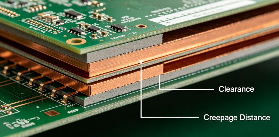
Practical Solutions for a Halogen-Free Workbench Setup
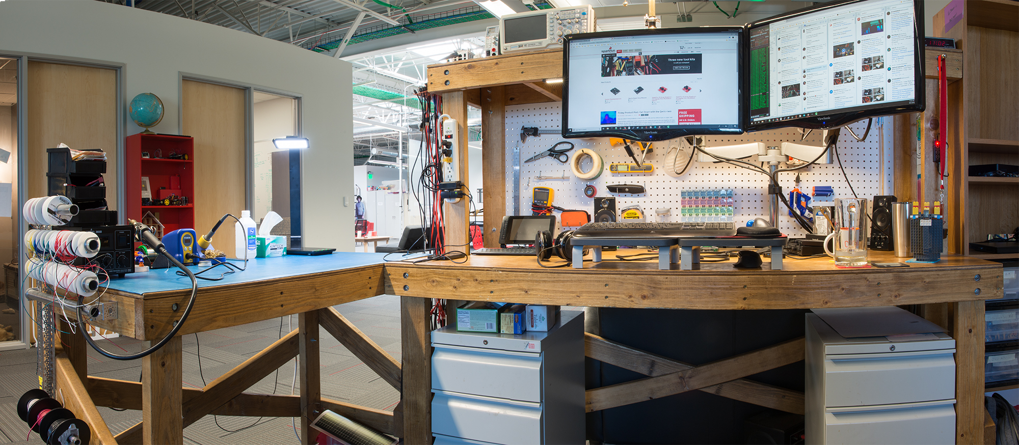
Start your eco-friendly electronics lab by selecting a sturdy workbench surface resistant to heat and spills, paired with ESD mats for component safety. Dedicate zones for assembly, testing, and storage to prevent cross-contamination. Source halogen-free PCBs as the foundation, verifying specs against industry definitions before ordering. Stock lead-free solder wire and pastes formulated without halogen activators, ensuring clean joints with minimal flux residue. Ventilation hoods or fans become essential, channeling any vapors away while maintaining a compact hobby lab footprint.
Assembly begins with proper tooling: adjustable soldering stations calibrated for lower temperatures compatible with halogen-free boards. Use fine-tip irons for precision on dense layouts, avoiding excessive heat that could stress phosphorus-based resins. Pre-bake components if needed, following moisture sensitivity guidelines to prevent reflow defects. For rework, opt for hot air tools with controlled profiles, testing joints visually and with multimeters for continuity.
Storage practices elevate sustainability: seal PCBs in moisture-barrier bags within anti-static bins, labeled clearly. Organize components by type, prioritizing halogen-free resistors, capacitors, and ICs marked accordingly per J-STD-609A guidelines. Waste management involves segregating scraps for specialized recycling, extending the lab's environmental electronics ethos. Regular audits ensure all supplies align with halogen-free criteria, fostering a consistent workflow.
Related Reading: Top 5 Misconceptions About Halogen Free PCB Manufacturing
Best Practices for Assembly and Maintenance in Your Hobby Lab
When populating boards, apply flux sparingly to leverage the inherent solderability of halogen-free finishes. Hand-soldering techniques shine here: tin tips frequently and use drag soldering for rows of pins, achieving IPC Class 2 acceptability without bridges. Inspect under magnification for voids, confirming fillet shapes meet visual criteria. For surface-mount work, stencil printing with low-residue pastes minimizes cleaning needs, preserving the halogen-free workbench's cleanliness.
Troubleshooting common issues starts with thermal profiling mockups. If delamination occurs, check preheat adequacy; halogen-free materials demand gradual ramps to avoid CTE mismatches. Multilayer stacks benefit from sequential baking, aligning with factory protocols for reliability. Maintenance involves wiping surfaces with isopropyl alcohol, avoiding halogen-containing cleaners that could introduce contaminants.
Expand capabilities with basic testing: continuity checks, insulation resistance meters, and thermal cameras spot hotspots early. Document processes in a lab notebook, noting material batches for traceability. These habits build a robust eco-friendly electronics lab, scalable for complex projects.
Related Reading: Improving Thermal Management in Halogen Free PCBs: Techniques and Materials
Long-Term Benefits and Insights for Hobbyists
Over time, a halogen-free workbench yields cost savings through durable materials and reduced rework. Fire safety improves markedly, with less corrosive smoke protecting gear during mishaps. Recyclability supports circular practices, allowing scrap repurposing in new prototypes. Insights from manufacturing reveal that consistent handling extends board life, ideal for iterative hobby designs.
Community sharing amplifies gains: document setups to inspire peers toward sustainable electronics. Challenges like higher initial material costs offset via bulk planning and yield improvements.
Conclusion
Building a sustainable electronics lab through the halogen-free approach empowers hobbyists with safe, effective workspaces. From material selection guided by standards to practical assembly routines, every step enhances environmental electronics. The halogen-free workbench not only mitigates risks but also aligns personal projects with industry sustainability. Embrace these practices for a greener, more reliable hobby lab today.
FAQs
Q1: What makes a PCB halogen-free for my eco-friendly electronics lab?
A1: Halogen-free PCBs limit chlorine and bromine to under 900 ppm each and total halogens below 1500 ppm, as defined by standards like IEC 61249-2-21. This ensures low toxicity in fires, ideal for home setups. Hobbyists verify via supplier datasheets, pairing with compatible fluxes for clean assembly. Such boards support sustainable electronics by improving recyclability and thermal performance.
Q2: How do I set up a halogen-free workbench safely?
A2: Designate zones for soldering, storage, and testing on a stable surface with ESD protection. Use lead-free, low-halogen solders and ensure ventilation captures residues. Stock certified halogen-free components, maintaining dry storage to prevent moisture issues. This creates a practical hobby lab focused on environmental electronics and fire safety.
Q3: Why choose halogen-free materials for hobby projects?
A3: They reduce toxic smoke emissions, enhancing safety in confined spaces while meeting environmental electronics goals. Phosphorus-based retardants offer comparable flame resistance with better insulation post-aging. Factory insights confirm reliability under rework, making them suitable for iterative prototyping without delamination risks.
Q4: Can halogen-free setups improve my sustainable electronics workflow?
A4: Yes, by simplifying waste segregation and recycling, plus durable boards that withstand multiple cycles. Align with standards for consistent quality, cutting long-term costs. Hobbyists gain a cleaner halogen-free workbench, boosting efficiency in prototyping.
References
IPC-4101E — Specification for Base Materials for Rigid and Multilayer Printed Boards. IPC, 2017
IEC 61249-2-21 — IEC 61249-2-21:2003. IEC, 2003
J-STD-609A — Marking and Labeling of Components, PCBs and PCB Assemblies. IPC/JEDEC, 2019