ALLPCB


Introduction
High-density interconnect (HDI) technology with microvias enables compact electronics designs essential for modern applications like smartphones, wearables, and medical devices. Engineers evaluating microvia PCB cost must weigh upfront expenses against long-term performance gains. While microvia PCBs command a premium over standard boards, their ability to support finer pitches and more layers justifies the investment in many scenarios. This article dissects microvia PCB manufacturing cost drivers, provides an HDI PCB cost comparison, and conducts a microvia PCB cost-benefit analysis to guide procurement and design decisions. Factory insights reveal how process choices influence pricing, helping electrical engineers optimize for reliability and efficiency. By aligning with industry standards, manufacturers ensure these boards meet demanding requirements without unnecessary cost escalation.
Understanding Microvia PCBs and Their Role in HDI Technology
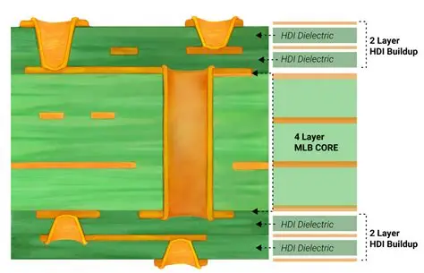
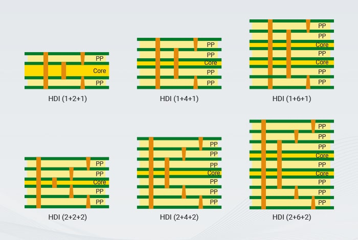
Microvias are small-diameter vias, typically under 150 microns, that connect layers in HDI PCBs without penetrating the entire board stack. Unlike through-hole vias in conventional multilayers, microvias allow for higher routing density and reduced board size. HDI structures are classified by buildup types such as 1+N+1, where microvias link outer layers to a core, or more complex 2+N+2 with staggered or stacked vias. These configurations support ball grid array (BGA) components with pitches below 0.5 mm, critical for high-performance electronics. As per IPC-2226A, design standards specify microvia aspect ratios and placement to ensure manufacturability. Electrical engineers benefit from HDI's shorter signal paths, which minimize inductance and improve integrity in high-speed circuits.
The relevance of microvia technology grows with miniaturization trends in consumer and industrial sectors. Standard PCBs struggle with dense layouts due to larger via sizes and spacing rules, leading to larger footprints. Microvia PCBs address this by enabling every-layer interconnects in advanced types, though they introduce unique fabrication challenges. Factory processes start with sequential lamination, building layers incrementally around a core substrate. This demands precise registration to align microvias across multiple cycles. Ultimately, microvia adoption matters for engineers aiming to fit more functionality into smaller spaces while maintaining signal quality.
Key Technical Principles of Microvia Formation and HDI Structures
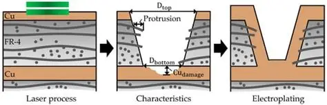
Microvias form primarily through laser ablation, which removes dielectric material with ultraviolet or CO2 lasers for diameters as small as 50 microns. Mechanical drilling suits larger vias but lacks precision for microvias, making laser the dominant method in HDI production. After drilling, vias require plating or filling with conductive epoxy to establish electrical continuity. Stacked microvias connect end-to-end across layers, while staggered ones offset for better reliability under thermal stress. These structures adhere to IPC-2226A guidelines on via capture pads and anti-pad sizes to prevent shorts. Engineers must consider via-in-pad designs, where components land directly on filled microvias, optimizing space but complicating rework.
Buildup processes involve multiple lamination, imaging, and etching cycles, each adding to complexity. For instance, in a 3+N+3 HDI, outer microvia layers laminate onto inner ones, requiring intermediate plating steps. Dielectric materials like resin-coated copper (RCC) or low-loss polymers support fine features but cost more than standard FR-4. Aspect ratios typically stay below 1:1 for reliable plating, influencing stack height limits. Thermal expansion mismatches between copper and dielectrics demand controlled curing to avoid cracks. These principles ensure HDI PCBs deliver superior electrical performance, with reduced parasitics enabling faster data rates.
Related Reading: Stacked vs. Staggered Microvias: Which Design is Right for Your PCB?
Microvia PCB Manufacturing Cost Drivers
Several factors drive microvia PCB cost, starting with the number of buildup layers and via structures. More sequential laminations mean additional handling, alignment, and yield risks, elevating expenses significantly. Laser drilling consumes time and consumables, with each microvia requiring precise energy control to avoid taper or residue. Via filling adds steps like electroplating or resin plug printing, followed by planarization via grinding or polishing. Complex stackups like any-layer HDI demand the most cycles, multiplying costs compared to simpler passive types.
Material selection influences pricing, as high-Tg dielectrics and thin cores prevent warpage in buildup. Tighter tolerances for line widths under 50 microns and spaces necessitate advanced exposure equipment and chemistry. Panel utilization drops with smaller features, increasing per-unit costs unless volumes compensate. Yield rates suffer from defects like via opens or plating voids, prompting extra inspections such as automated optical and electrical testing. Factory experience mitigates these through process controls, but initial setups for new designs incur non-recurring engineering fees. Understanding these microvia PCB manufacturing cost drivers empowers engineers to simplify designs without sacrificing density.
Board size and quantity further modulate costs, with prototypes commanding premiums due to setup overheads. High-volume runs amortize tooling, but HDI's specialized cleanrooms and equipment raise baseline rates. Environmental controls for laser operations and plating baths add operational expenses. Engineers can model costs by estimating buildup count and via density early in design.
Related Reading: Mastering Microvias: A Comprehensive Guide to PCB Laser Drilling
HDI PCB Cost Comparison with Standard Multilayer PCBs
Standard multilayer PCBs rely on mechanical drilling for through-vias, a faster and cheaper process than HDI's laser methods. A typical 8-layer standard board might use core-to-core lamination in one cycle, contrasting HDI's sequential builds. Through-vias span the full stack, consuming more copper and dielectric volume, yet fabrication yields higher due to fewer alignment steps. HDI introduces costs from intermediate processing, often 2-3 times higher per square inch for equivalent layer counts. However, HDI boards shrink overall dimensions, potentially reducing material use in compact applications.
Assembly costs diverge too, as HDI supports finer pitches with fewer vias obstructing routing. Standard boards require larger escape routing for BGAs, increasing layer needs. In an HDI PCB cost comparison, passive structures like 1+N+1 approach standard pricing at scale, while active any-layer types premium heavily. Factory data shows HDI's buildup elevates drill and plate times by factors of 4-5 per layer pair. Engineers trading size for cost might opt for blind vias in hybrids, bridging the gap. This comparison highlights HDI's value in density-constrained designs despite upfront premiums.
Microvia PCB Cost-Benefit Analysis and ROI Justification
Microvia PCB ROI emerges from performance edges offsetting higher fabrication costs. Smaller vias cut signal path lengths by up to 70 percent, slashing inductance for better high-speed integrity. This enables GHz operations without heavy equalization, reducing component counts and power draw. Board miniaturization trims enclosure sizes, material weights, and assembly footprints, yielding system-level savings. In wearables or automotive modules, HDI halves PCB area, amortizing costs over production volumes.
Reliability benefits include improved thermal dissipation via dense copper fills and shorter paths minimizing electromigration. J-STD-001 standards guide assembly to leverage these traits, ensuring robustness. Lifecycle ROI factors in fewer failures from signal crosstalk or EMI. For engineers, a microvia PCB cost-benefit analysis reveals breakeven at moderate volumes, especially where space dictates. Market differentiation through compact designs boosts competitiveness. Factories observe HDI's total cost of ownership drops below standards in high-mix scenarios.
Best practices like staggered vias over stacked reduce stress concentrations, enhancing yields. Design for testability with probe points on outer layers cuts validation expenses. Collaborating on stackups optimizes via counts. Volume commitments unlock discounts on setups.
Conclusion
Microvia PCB cost analysis underscores the strategic value of HDI in demanding applications. Key manufacturing cost drivers like buildup complexity and laser processes explain premiums, yet HDI PCB cost comparisons favor HDI for density needs. A thorough microvia PCB ROI evaluation, coupled with cost-benefit analysis, justifies investment through superior performance and miniaturization. Engineers should reference standards like IPC-2226A for compliant designs minimizing risks. By selecting appropriate structures and volumes, teams realize substantial returns. This approach positions HDI as essential for future-proof electronics.
FAQs
Q1: What are the primary microvia PCB manufacturing cost drivers?
A1: Laser drilling, sequential lamination, and via filling dominate costs due to precision equipment and yield-sensitive steps. Stacked structures add more cycles than staggered, while thin dielectrics raise material prices. Engineers mitigate by limiting buildup layers and standardizing tolerances. Factory alignment ensures compliance with process windows.
Q2: How does HDI PCB cost comparison stack up against standard PCBs?
A2: HDI incurs higher per-layer costs from buildup processes versus standard's single lamination. However, smaller sizes offset this in compact designs. Passive HDI nears standard pricing at volume, while complex types premium for density. Engineers balance via count and board area for optimal tradeoffs.
Q3: Is microvia PCB ROI positive for mid-volume production?
A3: Yes, through reduced system size, better signal integrity, and lower assembly needs. Breakeven occurs via material savings and performance gains. Microvia PCB ROI strengthens in high-speed apps minimizing rerouting layers. Standards guide reliable implementations boosting yields.
Q4: What best practices optimize microvia PCB cost-benefit analysis?
A4: Prioritize staggered vias, control aspect ratios per IPC-2226A, and model stackups early. Volume forecasting amortizes setups, while hybrid designs blend HDI with standard for hybrids. These yield balanced microvia PCB cost-benefit analysis favoring density-critical projects.
References
IPC-2226A — Sectional Design Standard for High Density Interconnect (HDI) Printed Boards. IPC, 2017
IPC-6012DS — Space and Military Avionics Applications Addendum to IPC-6012D, Qualification and Performance Specification for Rigid Printed Boards. IPC, 2015
J-STD-001 — Requirements for Soldered Electrical and Electronic Assemblies. IPC, 2020