 ALLPCB


Introduction
Mixed-signal PCBs integrate analog and digital circuits on a single board, combining high-speed digital processing with precise analog signal handling. These designs power applications like data acquisition systems, sensors, and communication modules where performance hinges on minimizing interference between domains. However, the proximity of noisy digital signals to sensitive analog paths often leads to crosstalk, ground bounce, and degraded signal integrity. A comprehensive mixed-signal PCB design checklist addresses these risks systematically, guiding engineers from schematic capture through fabrication. This structured approach reduces redesign iterations, cuts costs, and ensures reliable operation in demanding environments.
Engineers face unique challenges in mixed-signal layouts, such as partitioning sections effectively and managing power distribution without introducing noise. Without a rigorous checklist, common oversights like improper ground plane splits or inadequate decoupling can compromise functionality. The process spans pre-layout planning, detailed routing, verification, and manufacturability checks, each critical for success. By following a mixed-signal PCB design checklist, teams align design decisions with proven engineering principles. This article outlines key checklists tailored for electrical engineers, emphasizing logical steps to achieve optimal results. Ultimately, these practices bridge the gap between concept and production-ready boards.
What Is Mixed-Signal PCB Design and Why It Matters
Mixed-signal PCB design involves creating boards that accommodate both analog components, such as amplifiers and ADCs, and digital logic like microcontrollers and FPGAs. Analog sections require low-noise environments for accurate signal fidelity, while digital parts generate switching noise that can couple into sensitive traces. Effective designs isolate these domains through physical separation, dedicated power rails, and controlled impedance paths. Industry relevance grows with trends toward integrated systems-on-board, where space constraints amplify coupling risks. A PCB design review at multiple stages prevents issues that simulations alone might miss.
Checklists matter because mixed-signal boards demand precision beyond standard digital or analog layouts. Noise from digital clocks can raise analog distortion floors by orders of magnitude if unchecked. Pre-layout checklists catch schematic flaws early, while post-layout ones verify integrity. Following guidelines from IPC-2221C ensures trace widths, spacings, and layer usage support performance. Neglecting these steps leads to prototypes failing electromagnetic compatibility tests or field returns. For electrical engineers, checklists provide a repeatable framework, fostering consistency across projects and teams.
The economic impact underscores urgency; respins cost time and resources, delaying market entry. Structured checklists integrate design for manufacturability (DFM) early, aligning with fabrication capabilities. They also facilitate collaboration during PCB design reviews, where peers spot blind spots. In high-reliability sectors, adherence to such processes meets qualification needs under IPC-6012F. Overall, a mixed-signal PCB design checklist transforms complex challenges into manageable tasks, yielding robust, high-yield boards.
Pre-Layout Checklist: Building a Solid Foundation
The pre-layout phase focuses on schematic integrity and planning, forming the backbone of successful mixed-signal designs. Begin with a thorough schematic review to confirm all components match datasheets, including pinouts and values. Verify power budgets account for analog supply ripple requirements and digital transient currents. Plan partitioning by sketching analog, digital, and interface zones, ensuring physical separation exceeds 10% of board area for noisy sections. Define preliminary stackup with dedicated ground planes for each domain, calculating impedance targets based on signal speeds.
Component selection demands attention to noise specifications; choose op-amps with low input bias currents and ADCs with integrated drivers for mixed-signal paths. Check decoupling strategies, placing capacitors near every IC power pin with values spanning bypass to bulk. Review net classes for high-speed digital lines needing 50-ohm or 100-ohm differential routing. Ensure test points access critical nodes without compromising shielding. Document assumptions like operating temperatures to guide material choices compliant with IPC-2221C.
Power distribution planning prevents voltage droops; model PDN impedance early to size planes and vias. Confirm clock distribution minimizes skew for synchronous digital blocks interfacing analog. Simulate basic signal chains if tools allow, flagging potential bandwidth limits. Cross-check BOM for lead-free compatibility and thermal ratings. This pre-layout checklist minimizes layout rework, setting the stage for efficient routing.
A PCB design review here involves peers validating assumptions, often uncovering overlooked interactions like ADC sampling jitter from nearby logic. Update schematics with hierarchical sheets for clarity in complex designs. Finally, generate netlists and library checks to ensure footprint accuracy before import.
Key Layout Guidelines for Mixed-Signal PCBs
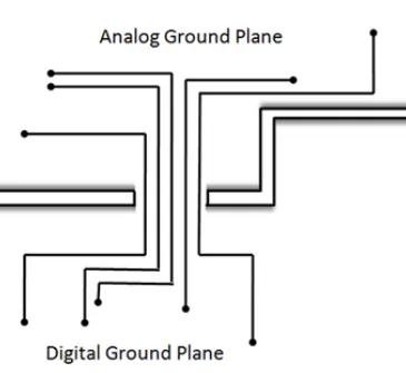
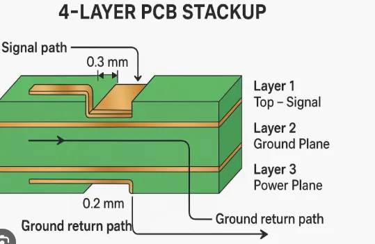
Once pre-layout is solid, layout begins with stackup definition, prioritizing signal integrity. Assign inner layers: top for analog components, bottom for digital, with split grounds on layer 2 and 3 connected via a narrow bridge under the ADC. Maintain symmetric stackup for minimal warpage, using low-loss dielectrics for high-frequency analog. Place sensitive analog ICs near board edges or connectors to shorten input traces. Group digital logic centrally, away from analog sections by at least 5 mm.
Component placement follows functional blocks; keep bypass caps within 1 mm of pins, routing short, wide paths. Avoid vias in analog signal paths where possible to preserve integrity. During routing, segregate traces: analog on dedicated layers, digital on others, with no orthogonals crossing splits. Use guard rings around analog traces, grounding them to shield from fields. For high-speed digital, length-match clocks and implement via fencing for return paths.
Power routing employs wide planes split by domain, with ferrite beads at interfaces if decoupling proves insufficient. Monitor clearance rules per IPC-2221C, increasing for high-voltage analog sections. Iteratively check for acute angles that form antennas. This during-layout discipline ensures the board embodies pre-planned isolation.
Related Reading: Power Integrity in Mixed Signal PCBs: Minimizing Noise and Ensuring Stability
Post-Layout Checklist: Verification and Optimization
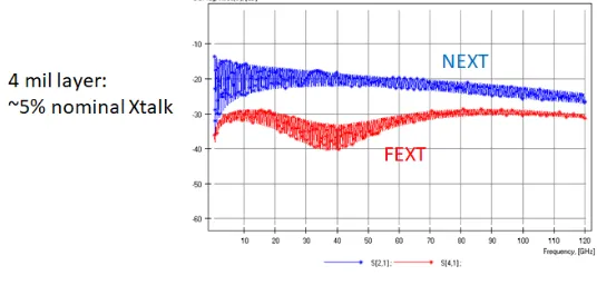
Post-layout verification confirms the design meets intent through multiple lenses. Run design rule checks (DRC) for all clearances, annular rings, and plane stitching. Perform layout vs. schematic (LVS) to catch netlist discrepancies. Analyze signal integrity: check return path continuity, impedance profiles, and crosstalk budgets using field solvers. Review thermal hotspots via simulation, ensuring vias dissipate heat from power devices.
Examine ground splits; confirm no digital traces cross analog planes without stitching caps. Verify decoupling efficacy by probing PDN impedance curves. Check high-speed nets for length matching within 10% of bit time. Inspect silkscreen for clarity, avoiding overlap with pads. Generate fabrication drawings with stackup details, drill tables, and panelization notes.
A thorough PCB design review post-layout includes blind reviews by colleagues, focusing on edge cases like EMI escape paths. Simulate full-board eye diagrams for critical interfaces. Optimize rerouting for slivers or islands that risk fab defects. This post-layout checklist catches 90% of issues before tape-out.
Design for Manufacturability (DFM) Checklist: Bridging to Fabrication
DFM ensures the design fabricates reliably without yield loss. Verify minimum trace widths and spacings per fab capabilities, typically 4 mil for Class 3. Check via annular rings exceed 3 mil external, with no necking. Confirm solder mask expansion prevents bridging, at least 3 mil over copper. Inspect for acid traps: smooth inner corners on polygons above 45 degrees.
Review drill sizes; standardize to 0.1 mm increments, avoiding slivers between holes under 0.15 mm. Ensure copper balance within 10% per layer to prevent plating voids. Define fab notes clearly: surface finish, legend colors, and impedance control tolerances. Panelization accounts for fiducials and v-scoring if needed.
IPC-6012F guides acceptance criteria, emphasizing bow and twist limits under 0.75%. Simulate warpage for asymmetric stacks. Check silkscreen polarity marks and assembly aids. Final DFM checklist submission prompts fab feedback, refining for first-pass success.
Related Reading: DFM Pitfalls to Avoid in Mixed-Signal PCB Layout
Conclusion
A mixed-signal PCB design checklist streamlines the journey from schematic to fabrication, mitigating risks inherent to dual-domain integration. Pre-layout planning establishes isolation foundations, layout enforces separation, post-layout verifies performance, and DFM secures producibility. Integrating PCB design reviews at each stage amplifies quality. Adhering to IPC standards like IPC-2221C and IPC-6012F guarantees compliance and reliability. Electrical engineers benefit from this structured method, delivering boards that perform under real-world stresses. Implement these checklists to elevate design outcomes consistently.
FAQs
Q1: What is a mixed-signal PCB design checklist?
A1: A mixed-signal PCB design checklist is a systematic set of verification steps spanning schematic review, layout, and fabrication for boards combining analog and digital circuits. It addresses noise isolation, partitioning, and signal integrity to prevent common failures like crosstalk. Key sections include pre-layout component checks and post-layout DRCs. Following it reduces respins by ensuring domain separation and compliance with standards like IPC-2221C. This tool empowers engineers to achieve high-yield prototypes efficiently.
Q2: Why perform a pre-layout checklist in mixed-signal designs?
A2: The pre-layout checklist validates schematics, power planning, and partitioning before routing commits resources. It identifies issues like inadequate decoupling or mismatched impedances early, avoiding costly layout changes. For mixed-signal boards, it confirms analog-digital separation plans and net classes. This step aligns with PCB design review best practices, saving time and enhancing signal fidelity from the start.
Q3: What does a post-layout checklist cover for PCB design review?
A3: A post-layout checklist includes DRC, LVS, signal integrity analysis, and thermal reviews to confirm layout fidelity. In mixed-signal contexts, it verifies ground splits, trace isolation, and PDN performance. It flags fab risks like slivers or mask bridges. Conducting this during PCB design review ensures the board meets performance specs before DFM handover.
Q4: How does design for manufacturability (DFM) fit into mixed-signal PCB checklists?
A4: DFM checklists focus on fabrication viability, checking annular rings, copper balance, and mask rules per IPC-6012F. For mixed-signal boards, they ensure impedance-controlled traces and plane splits survive plating. Integrating DFM early prevents yield issues from complex routing. This final checklist bridges design to production seamlessly.
References
- IPC-2221C - Generic Standard on Printed Board Design. IPC, 2023
- IPC-6012F - Qualification and Performance Specification for Rigid Printed Boards. IPC, 2023
- IPC-A-600M - Acceptability of Printed Boards. IPC, 2025


