 ALLPCB


Introduction
Halogen-free PCBs have become standard in modern electronics due to environmental regulations and safety concerns during manufacturing and end-use. These boards replace traditional brominated flame retardants with alternatives like phosphorus or nitrogen-based systems, aligning with sustainability goals. However, this shift often introduces challenges in thermal management because the new resin formulations can exhibit different thermal properties compared to conventional materials. Effective heat dissipation remains critical for reliability in applications such as power supplies, automotive electronics, and high-density designs where component operating temperatures must stay within safe limits. Engineers must employ targeted techniques and material selections to optimize halogen-free PCB thermal management without compromising performance. This article explores proven methods to enhance heat dissipation, focusing on thermal vias, metal core PCB structures, and materials with improved thermal conductivity.
Understanding Halogen-Free PCBs and the Need for Thermal Management
Halogen-free PCBs are defined by industry specifications that limit chlorine and bromine content to ensure reduced toxicity in combustion byproducts. These materials meet requirements outlined in standards like IPC-4101B for base materials used in rigid and multilayer boards. While they offer advantages in recyclability and worker safety, their thermal performance can lag behind halogenated counterparts due to variations in filler content and resin chemistry. In high-power circuits, poor heat dissipation leads to elevated junction temperatures, accelerating degradation mechanisms such as electromigration and delamination. Thermal management ensures that halogen-free PCB thermal management supports longer service life and compliance with performance classes in demanding environments. Engineers prioritize this aspect during design to prevent failures in densely packed assemblies.
The relevance intensifies in sectors like telecommunications and renewable energy, where power densities continue to rise. Without adequate strategies, hotspots form around ICs, resistors, and power transistors, reducing overall system efficiency. Proper thermal design not only mitigates risks but also allows for smaller form factors by maximizing the heat spreading capability of the board itself. Key metrics include thermal resistance from junction to ambient and the coefficient of thermal expansion mismatch between layers.
Thermal Challenges and Principles in Halogen-Free PCBs
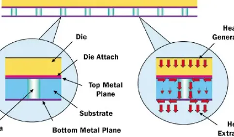
Heat generation in PCBs primarily stems from Joule heating in conductors and power dissipation in components. In halogen-free laminates, the dielectric layers typically exhibit lower in-plane and through-plane thermal conductivity because alternative flame retardants may not integrate as effectively with conductive fillers. Conduction through the board follows Fourier's law, where heat flux is proportional to the thermal conductivity gradient. Copper planes provide excellent lateral spreading, but vertical heat transfer through the core material becomes the bottleneck in multilayer stacks. Radiation and convection from surfaces play secondary roles unless augmented by external aids.
Warpage and CTE differences exacerbate issues during thermal cycling, potentially cracking vias or lifting pads. Halogen-free resins often have higher moisture absorption, which further degrades thermal stability under humidity. Understanding these mechanisms guides the selection of countermeasures. For instance, the z-axis thermal conductivity governs heat flow from inner layers to the surface, making material choice pivotal.
Key Techniques for Enhancing Heat Dissipation
Thermal vias serve as efficient conduits for vertical heat transfer, bridging copper planes across dielectric layers. Arrays of these vias, placed strategically under heat-generating components, create low-resistance thermal paths to outer layers or ground planes. Plated vias enhance conductivity, while filled variants using conductive epoxy or solder paste minimize voids and improve reliability. Diameter, pitch, and aspect ratio must balance thermal performance with fabrication feasibility to avoid drill breakout or plating defects.
Increasing copper thickness in power and ground planes boosts in-plane thermal conductivity, facilitating radial heat spreading. Wider traces and polygons under hotspots further aid this process. Combining these with embedded heat spreaders or coins made of copper slugs pressed into the board elevates overall dissipation. Surface treatments like thermal pads or direct heatsink attachment complete the strategy.
Advanced Materials for Superior Thermal Conductivity
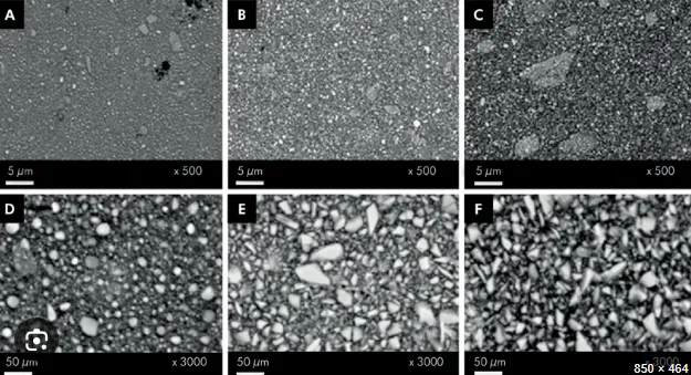
Selecting laminates with ceramic or metal oxide fillers, such as alumina or boron nitride, significantly raises thermal conductivity in halogen-free systems. These fillers create percolating networks that enhance phonon transport through the resin matrix without introducing halogens. High-frequency formulations often incorporate such additives to meet both electrical and thermal demands. Engineers evaluate materials based on through-plane and in-plane values to predict board-level performance.
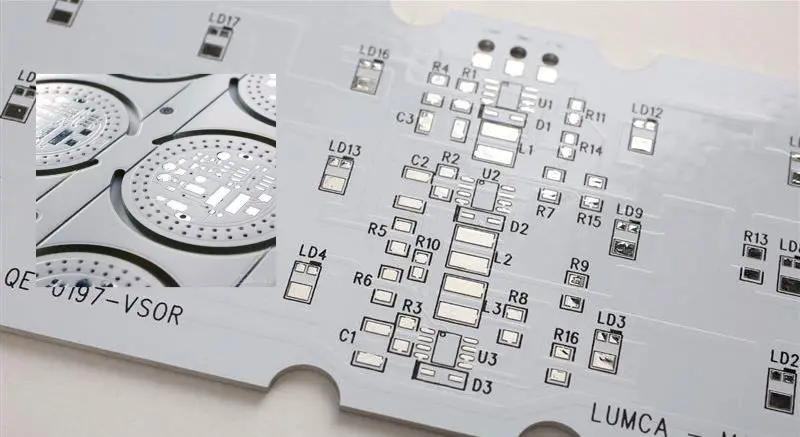
Metal core PCBs represent a robust solution for extreme heat loads, featuring an aluminum or copper core sandwiched between insulating dielectric and circuit layers. The core acts as a heat sink, channeling dissipation to external chassis or fins. This structure excels in LED lighting and power modules, where uniform temperature distribution prevents hotspots. Compatibility with halogen-free dielectrics ensures environmental compliance while delivering superior thermal management.
Best Practices in Design and Manufacturing for Halogen-Free PCB Thermal Management
Design workflows begin with thermal simulations using finite element analysis to model junctions, vias, and ambient conditions. Place high-power components over via fields and solid copper pours, adhering to guidelines in IPC-2221B for printed board design. Minimize layer count where possible to shorten vertical paths, and incorporate blind or buried vias for precision. Stackup planning ensures symmetric builds to control warpage.
Manufacturing processes demand controlled lamination cycles to preserve filler alignment and avoid microcracks. Via filling techniques, such as vacuum-assisted epoxy injection, enhance robustness under thermal stress. Qualification per IPC-6012 standards verifies performance through thermal cycling and shock tests. Post-assembly
Troubleshooting common issues involves identifying delamination via acoustic microscopy or infrared thermography. If hotspots persist, iterate via density or filler type. Collaboration between design and fabrication teams ensures alignment with class 3 requirements for high-reliability applications.
Conclusion
Optimizing halogen-free PCB thermal management requires a multifaceted approach combining material innovation, structural enhancements, and precise design practices. Techniques like thermal vias and metal core PCB configurations, paired with high thermal conductivity laminates, effectively address dissipation challenges. Adhering to established standards ensures reliability across thermal cycles. Electrical engineers can achieve balanced performance by prioritizing simulation-driven layouts and rigorous qualification. These strategies not only extend component life but also support compact, efficient electronics in a halogen-restricted world.
FAQs
Q1: What role do thermal vias play in halogen-free PCB thermal management?
A1: Thermal vias provide low-impedance paths for heat to travel vertically through the stackup, connecting inner copper layers to surface dissipators. In halogen-free boards, where dielectric thermal conductivity is moderate, via arrays under components reduce peak temperatures by distributing heat evenly. Proper plating and filling prevent reliability issues during reflow or operation. Design them with 0.2 to 0.3 mm diameters in grids for optimal flow without excessive cost.
Q2: How does a metal core PCB improve heat dissipation?
A2: A metal core PCB uses a thick metallic base, typically aluminum, to rapidly conduct heat away from circuits via an insulating dielectric layer. This excels in high-power halogen-free applications by lowering thermal resistance to chassis-mounted heatsinks. The core spreads heat laterally far better than standard FR-4 cores. It suits power electronics where uniform temperatures prevent failures.
Q3: Why is thermal conductivity critical in material selection for halogen-free PCBs?
A3: Thermal conductivity determines how efficiently heat moves through the laminate, preventing hotspots in dense designs. Halogen-free resins with conductive fillers like ceramics offer higher values than unfilled epoxies, aiding overall board dissipation. Engineers select based on z-axis performance for multilayer heat paths. This ensures compliance with reliability specs under load.
Q4: What are best practices for implementing thermal vias in heat dissipation?
A4: Position via arrays directly beneath hotspots, using 4-8 vias per square millimeter spaced at 0.5 mm pitch. Fill with conductive paste for robustness, and connect to full ground planes. Simulate to verify temperature drops, and qualify via thermal cycling tests. This maximizes effectiveness in halogen-free PCB thermal management.
References
IPC-4101B - Specification for Base Materials for Rigid and Multilayer Printed Boards. IPC, 2006
IPC-2221B - Generic Standard on Printed Board Design. IPC, 2012
IPC-6012D - Qualification and Performance Specification for Rigid Printed Boards. IPC, 2015


