 ALLPCB


If you're an electrical engineer working on high-speed designs, you might be wondering how to optimize PCB lamination for signal integrity and performance. The answer lies in selecting the right materials, mastering stack-up design, and applying proven lamination techniques tailored for high-frequency applications. In this blog, we dive deep into the world of high-speed PCB lamination, exploring key considerations like impedance control, low-loss laminates, and manufacturing practices to ensure your designs meet the demands of modern electronics. Let’s break it down step by step to help you achieve reliable and efficient high-speed PCBs.
Introduction to High-Speed PCB Lamination
High-speed PCB designs are the backbone of modern electronics, powering everything from 5G communications to high-performance computing. As data rates climb into the gigabits per second (Gbps) range and frequencies reach tens of gigahertz (GHz), the role of PCB lamination becomes critical. Lamination isn’t just about bonding layers together; it’s about ensuring signal integrity, controlling impedance, and minimizing losses in high-frequency PCB manufacturing.
For engineers, the challenge is clear: how do you create a PCB that supports lightning-fast signal transmission without distortion or interference? The solution starts with understanding the lamination process and its impact on performance. This blog will guide you through the essential techniques and considerations for high-speed PCB lamination, helping you make informed decisions for your next project.
What is PCB Lamination and Why Does It Matter for High-Speed Designs?
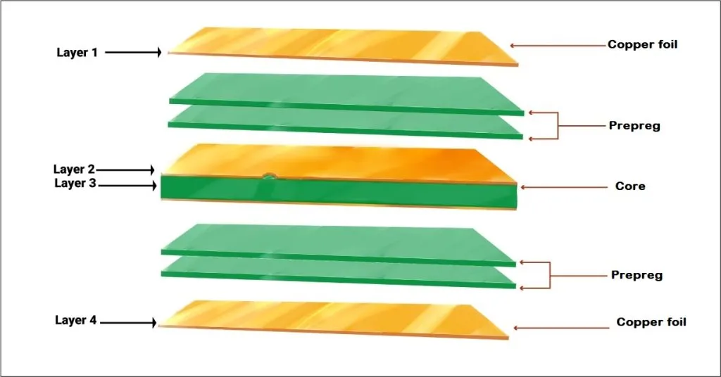
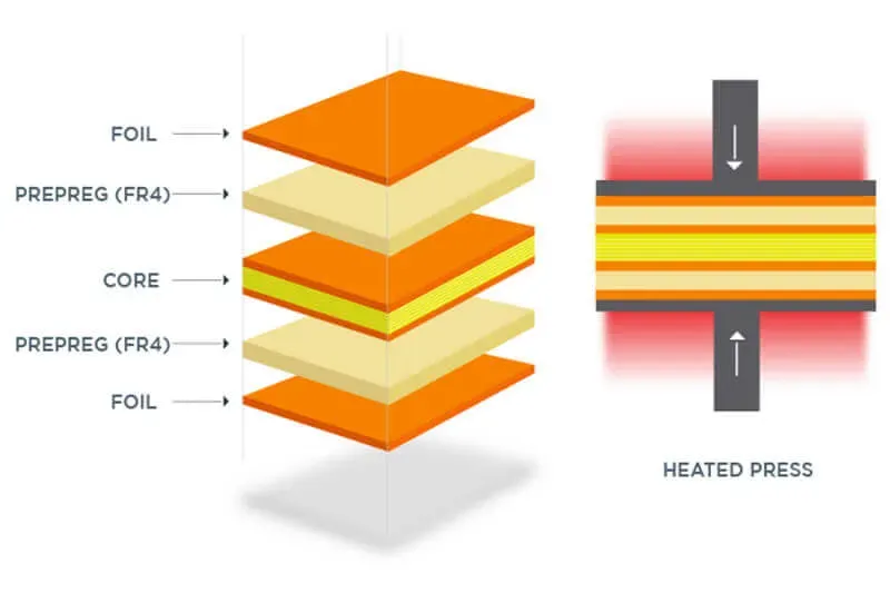
PCB lamination is the process of bonding multiple layers of materials—such as copper foil, dielectric substrates, and prepreg (pre-impregnated resin)—into a single, solid board using heat and pressure. In high-speed designs, this process directly affects how signals travel through the board. Poor lamination can lead to issues like signal loss, crosstalk, and impedance mismatches, which are disastrous at high frequencies.
For example, in a 10 Gbps data transmission system, even a slight variation in dielectric thickness or material properties during lamination can cause signal delays or reflections. That’s why high-speed PCB lamination requires precision and attention to material selection, layer alignment, and manufacturing techniques. Let’s explore the key factors that make lamination a cornerstone of high-frequency performance.
Signal Integrity in High-Speed PCB Lamination
Signal integrity refers to the quality of an electrical signal as it travels through a PCB. In high-speed designs, maintaining signal integrity is non-negotiable. During lamination, factors like dielectric constant (Dk) consistency and layer alignment play a huge role. If the dielectric material varies across the board, signals can experience different propagation delays, leading to timing errors.
One common issue is the fiber weave effect, where the fiberglass weave in the laminate affects the dielectric constant under high-speed traces. This can cause one trace in a differential pair to travel faster than the other, skewing the signal. To mitigate this, engineers often use low-loss laminates with uniform weave patterns or rotate trace routing to avoid alignment with the weave direction.
Impedance Control Through Lamination
Impedance control is critical for high-speed designs, ensuring that signals encounter consistent resistance as they travel through traces. In a typical high-speed PCB, target impedance might be 50 ohms for single-ended traces or 100 ohms for differential pairs. Lamination impacts impedance by determining the thickness and uniformity of dielectric layers between conductive traces.
For instance, if a dielectric layer is unevenly pressed during lamination, the spacing between a trace and its reference plane changes, altering impedance. This can lead to signal reflections and data errors. To achieve tight impedance control (often within ±5% tolerance), manufacturers must use precise lamination processes and materials with stable Dk values, typically in the range of 2.2 to 4.5 for high-speed applications.
Key Techniques for High-Speed PCB Lamination
Creating a high-performance PCB for high-speed applications requires specialized lamination techniques. Below, we outline the most important methods to ensure your board meets the demands of high-frequency signals.
1. Sequential Lamination for Complex Stack-Ups
Sequential lamination is often used in high-speed designs with complex stack-ups (e.g., 8 or more layers). This technique involves laminating subsets of layers separately before combining them into the final board. It’s especially useful for boards with buried or blind vias, which are common in high-density interconnect (HDI) designs for high-speed applications.
The benefit? Sequential lamination reduces alignment errors and stress on inner layers, ensuring consistent dielectric spacing for impedance control. However, it’s a more expensive and time-consuming process, so it’s typically reserved for critical designs like those in telecommunications or aerospace.
2. Vacuum Lamination for Uniform Pressure
In high-speed PCB manufacturing, vacuum lamination is a game-changer. By removing air from the lamination chamber, this technique ensures even pressure distribution across the board, preventing voids or resin starvation in the prepreg. Voids can disrupt signal paths and cause failures in high-frequency designs, so vacuum lamination is often a must for boards operating above 5 GHz.
3. Controlled Heating and Cooling Cycles
During lamination, the heating and cooling cycles must be carefully controlled to avoid warping or delamination. For high-speed PCBs, manufacturers often use gradual temperature ramps (e.g., 2-3°C per minute) to minimize thermal stress on low-loss laminates. This ensures the board remains flat and stable, which is crucial for maintaining signal integrity over long traces.
Stack-Up Design: Building the Foundation for High-Speed Performance
Stack-up design is the blueprint of your PCB, defining how layers of copper and dielectric materials are arranged. A well-designed stack-up is essential for high-speed PCB lamination, as it directly impacts signal integrity, impedance, and electromagnetic interference (EMI).
Balancing Signal and Power Layers
In a typical high-speed PCB stack-up, signal layers are sandwiched between ground planes to provide a consistent return path and reduce crosstalk. For example, a 6-layer stack-up might look like this:
- Layer 1: Signal (Top)
- Layer 2: Ground
- Layer 3: Signal
- Layer 4: Power
- Layer 5: Ground
- Layer 6: Signal (Bottom)
This arrangement minimizes loop inductance and ensures stable impedance for high-speed signals. Engineers must also balance the stack-up symmetrically to prevent warping during lamination, which can distort signal paths.
Dielectric Thickness and Material Selection
The thickness of dielectric layers in the stack-up affects both impedance and signal speed. For high-speed designs, thinner dielectrics (e.g., 3-5 mils) are often used between signal and ground layers to achieve tighter coupling and lower impedance. However, this requires precise lamination to avoid inconsistencies.
Material selection is equally important. Low-loss laminates like Rogers RO3003 (Dk of 3.0, loss tangent of 0.0010 at 10 GHz) or Isola I-Speed (Dk of 3.6, loss tangent of 0.006 at 10 GHz) are popular choices for high-frequency PCB manufacturing. These materials minimize signal attenuation, making them ideal for applications above 5 GHz.
Choosing Low-Loss Laminates for High-Frequency Designs
Material selection is at the heart of high-speed PCB lamination. Low-loss laminates are specifically engineered to reduce signal attenuation and dielectric losses at high frequencies. But with so many options, how do you choose the right one?
Key Properties of Low-Loss Laminates
When selecting a laminate for high-frequency PCB manufacturing, focus on these properties:
- Dielectric Constant (Dk): A lower Dk (e.g., 2.2-3.5) allows signals to travel faster and reduces crosstalk. Materials like PTFE-based laminates often have Dk values in this range.
- Loss Tangent (Df): This measures energy loss in the material. For high-speed designs, aim for a loss tangent below 0.005 at your operating frequency. For example, Rogers RO4350B has a loss tangent of 0.0037 at 10 GHz.
- Thermal Stability: High-speed PCBs often operate in demanding environments. Choose laminates with a high glass transition temperature (Tg), such as 180°C or above, to withstand lamination and soldering processes.
Popular Low-Loss Materials for High-Speed PCBs
Some widely used low-loss laminates include:
- Rogers RO3000 Series: Ideal for RF and microwave applications up to 40 GHz, with Dk values around 3.0 and ultra-low loss tangents.
- Isola Astra MT77: Offers a Dk of 3.0 and loss tangent of 0.0017 at 10 GHz, perfect for 5G and automotive radar designs.
- Nelco N4000-13 EP: A cost-effective option with a Dk of 3.7 and good performance up to 10 GHz.
Choosing the right material often involves balancing performance with cost. For extremely high-frequency designs (e.g., above 20 GHz), premium materials like Rogers are worth the investment. For less demanding applications, FR-4 variants with improved loss characteristics might suffice.
Manufacturing Considerations for High-Speed PCB Lamination
Even the best design can fail if manufacturing isn’t executed properly. High-frequency PCB manufacturing requires strict process controls during lamination to ensure consistency and reliability. Here are some key considerations:
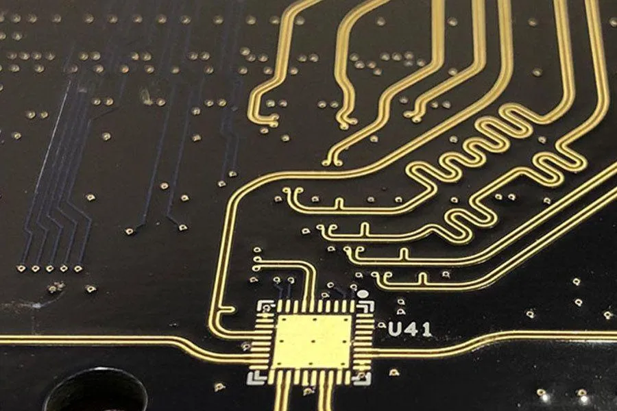
Layer Registration and Alignment
In high-speed designs, even a 1-mil misalignment between layers can disrupt impedance and signal paths. Manufacturers use optical alignment systems and X-ray inspection to ensure precise registration during lamination. This is especially critical for HDI boards with fine-pitch vias.
Resin Flow and Void Prevention
During lamination, resin from the prepreg must flow evenly to fill gaps and bond layers without creating voids. Voids can act as weak points, causing signal loss or mechanical failure. Using vacuum lamination and optimizing resin content (typically 50-60% in prepreg) helps achieve a void-free board.
Post-Lamination Testing
After lamination, high-speed PCBs undergo rigorous testing to verify performance. Time-domain reflectometry (TDR) is often used to measure impedance, ensuring it falls within the target range (e.g., 50 ± 2.5 ohms). Additionally, cross-sectional analysis can reveal issues like delamination or uneven dielectric thickness.
Common Challenges in High-Speed PCB Lamination and How to Overcome Them
Despite best efforts, challenges can arise during high-speed PCB lamination. Here are some common issues and practical solutions:
- Delamination: Caused by poor adhesion or thermal stress. Use compatible materials with similar coefficients of thermal expansion (CTE) and control lamination temperatures.
- Signal Skew: Often due to the fiber weave effect. Route critical traces at an angle (e.g., 10-15 degrees) to the weave or use spread-glass laminates for uniformity.
- Warping: Results from uneven stack-ups or rapid cooling. Design symmetrical stack-ups and use gradual cooling cycles during lamination.
Conclusion: Building Better High-Speed PCBs Through Lamination
High-speed PCB lamination is both an art and a science, requiring careful attention to materials, techniques, and manufacturing processes. By focusing on signal integrity, impedance control, stack-up design, and low-loss laminates, you can create PCBs that meet the rigorous demands of high-frequency applications. Whether you’re designing for 5G, automotive radar, or data centers, the right lamination approach can make all the difference.
As an electrical engineer, your next step is to collaborate closely with your PCB manufacturer to select the best materials and processes for your design. Test early, iterate often, and don’t shy away from investing in premium laminates if your application demands it. With these strategies, you’ll be well-equipped to tackle the challenges of high-speed PCB design and deliver reliable, high-performance boards.


