 ALLPCB


Printed Circuit Boards (PCBs) are the backbone of modern electronics, powering everything from smartphones to industrial machinery. However, even the most meticulously designed PCBs can fail, leading to costly downtime, reduced performance, or complete device failure. Understanding the root causes of PCB failures and how to address them is critical for engineers striving to ensure reliability and longevity in their designs. In this blog, we dive deep into PCB failure analysis, exploring common issues, diagnostic techniques, and preventive strategies to help you build robust, high-performing circuits.
Whether you're troubleshooting a prototype or optimizing a production run, this guide provides actionable insights to identify and resolve PCB failures effectively. Let's explore the key failure modes, analysis methods, and best practices to keep your circuits running smoothly.
Why PCB Failure Analysis Matters
PCB failures can disrupt operations, increase costs, and damage reputations. A single failure in a mission-critical system—like an automotive control unit or medical device—can have severe consequences, including safety risks. Failure analysis is the systematic process of identifying the cause of a PCB malfunction, pinpointing defects, and implementing corrective actions. By understanding failure modes and their origins, engineers can improve design reliability, reduce rework, and enhance product performance.
Failure analysis isn't just about fixing a broken board; it's about learning from mistakes to prevent future issues. With the increasing complexity of modern PCBs—featuring high-density interconnects, lead-free soldering, and multi-layer designs—thorough analysis is more important than ever.
Common PCB Failure Modes
To effectively troubleshoot a PCB, you must first understand the most common failure modes. Below, we outline the primary issues engineers encounter, along with their causes and symptoms.
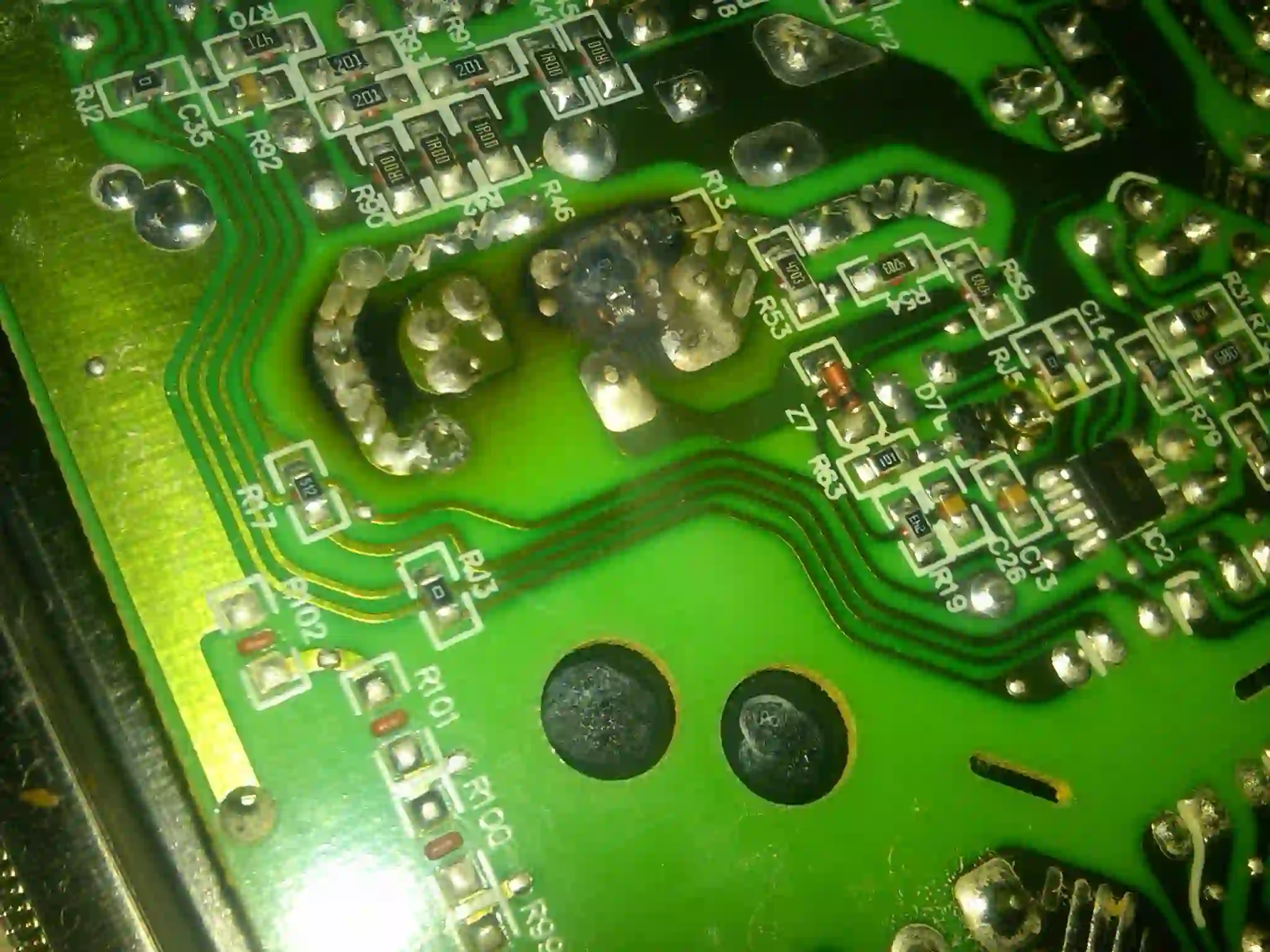
1. Solder Joint Failures
Solder joints are critical for connecting components to the PCB. Failures here are among the most common issues, often caused by:
- Thermal Stress: Repeated heating and cooling cycles can cause solder joints to crack. For example, a solder joint subjected to temperature swings from -40°C to 85°C may develop micro-cracks after 1,000 cycles.
- Poor Soldering Practices: Excessive or insufficient solder, cold joints, or improper reflow temperatures (e.g., exceeding 260°C for lead-free solder) can weaken connections.
- Vibration: In high-vibration environments, such as automotive applications, solder joints may fatigue and fail.
Symptoms: Intermittent connections, open circuits, or complete component failure.
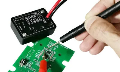
2. Open and Short Circuits
- Open Circuits: Occur when a conductive path is broken, preventing current flow. Causes include damaged traces (e.g., from mechanical stress), lifted pads, or incomplete soldering. For instance, a trace with a width of 0.1 mm may break under excessive flexing.
- Short Circuits: Happen when unintended connections form between conductive paths, often due to solder bridges, manufacturing defects, or contamination. A short between two 0.5 mm-pitched traces can cause overheating or component burnout.
Symptoms: Device malfunctions, overheating, or total failure.
Recommended Reading: Detecting Short Circuits in PCBs: Tools and Techniques
3. Component Failures
Components like resistors, capacitors, or ICs can fail due to:
- Electrical Overstress: Overvoltage (e.g., a 5V IC exposed to 12V) or overcurrent can burn out components.
- Defective Parts: Low-quality or counterfeit components may fail prematurely.
- Aging: Capacitors, for example, may degrade after 5–10 years, reducing capacitance (e.g., from 10 µF to 8 µF).
Symptoms: Erratic behavior, reduced performance, or non-functional circuits.
4. Signal Integrity Issues
High-speed PCBs are particularly susceptible to signal integrity problems, such as:
- Impedance Mismatch: A trace with an impedance of 50 ohms mismatched to a 75-ohm load can cause signal reflections, degrading performance.
- Crosstalk: Closely spaced traces (e.g., 0.2 mm apart) can induce unwanted signals, especially at frequencies above 1 GHz.
- EMI/EMC Interference: External electromagnetic interference or poor grounding can distort signals.
Symptoms: Data errors, reduced signal quality, or system crashes.
5. Environmental Damage
PCBs exposed to harsh conditions may fail due to:
- Moisture: Humidity levels above 85% can cause corrosion or conductive anodic filament (CAF) formation, leading to leakage currents.
- Temperature Extremes: Operating beyond a PCB's rated temperature (e.g., above 125°C) can warp boards or degrade materials.
- Contamination: Dust or ionic residues (e.g., from flux) can cause shorts or corrosion.
Symptoms: Gradual performance degradation or sudden failure.
PCB Failure Analysis Techniques
Once a failure is identified, engineers use a combination of non-destructive and destructive techniques to diagnose the root cause. Here are the most effective methods:
1. Visual Inspection
The first step in failure analysis is a thorough visual inspection using tools like:
- Stereomicroscopes: Magnification up to 40x reveals surface defects like solder bridges or burnt components.
- Metallurgical Microscopes: Higher magnification (up to 1000x) identifies micro-cracks or contamination.
Example: A visual inspection might reveal a solder bridge between two 0.4 mm-pitched pins, causing a short circuit.
2. X-Ray Inspection
Non-destructive X-ray imaging examines internal structures, such as:
- Solder Joint Integrity: Detects voids or cracks in Ball Grid Array (BGA) components.
- Via Failures: Identifies barrel cracking in plated through-holes (PTHs).
Example: An X-ray might show a 20% void in a BGA solder ball, indicating a weak joint.
3. Scanning Electron Microscopy (SEM)
SEM provides high-resolution images (up to 100,000x magnification) and elemental analysis to study:
- Microstructural Defects: Corrosion or solder joint fatigue.
- Contamination: Identifies residues like flux or ionic contaminants.
Example: SEM might reveal chlorine residues from flux, causing corrosion on a copper trace.
4. Cross-Sectioning
This destructive technique involves slicing the PCB to examine internal structures, such as:
- Solder Joint Quality: Checks for cracks or voids.
- Plating Thickness: Ensures copper plating in vias meets specifications (e.g., 25 µm minimum).
Example: Cross-sectioning might show a 10 µm crack in a PTH barrel, indicating thermal fatigue.
5. Electrical Testing
Electrical tests, such as continuity testing or in-circuit testing (ICT), diagnose:
- Open/Short Circuits: Measures resistance to detect breaks or unintended connections.
- Signal Integrity: Uses oscilloscopes to verify signal quality (e.g., rise time of 1 ns).
Example: ICT might detect a 100-ohm resistance in a trace expected to be 0 ohms, indicating an open circuit.
6. Thermal Analysis
Techniques like thermal imaging or thermocouples identify overheating issues, such as:
- Hot Spots: Components exceeding 150°C may indicate poor thermal management.
- Thermal Stress: Uneven heating can cause board warping.
Example: Thermal imaging might reveal a capacitor operating at 160°C, exceeding its 125°C rating.
Preventing PCB Failures
While failure analysis is essential for troubleshooting, preventing issues during design and manufacturing is even better. Here are proven strategies to enhance PCB reliability:
1. Design for Reliability (DfR)
- Trace Routing: Ensure controlled impedance (e.g., 50 ohms for high-speed signals) and adequate trace width (e.g., 0.2 mm for 1A current).
- Component Placement: Maintain spacing (e.g., 0.5 mm minimum) to prevent overheating or crosstalk.
- Ground Planes: Use continuous ground planes to reduce EMI and improve signal integrity.
2. Material Selection
- High-Quality Laminates: Choose materials like FR-4 with a high glass transition temperature (Tg > 170°C) for thermal stability.
- Surface Finishes: Select finishes like ENIG (Electroless Nickel Immersion Gold) for reliable solderability and corrosion resistance.
3. Robust Manufacturing Processes
- Cleanliness: Maintain ionic contamination below 1.56 µg/cm² (per IPC-TM-650) to prevent corrosion.
- Soldering Standards: Follow IPC-A-610 guidelines for acceptable solder joints, ensuring reflow temperatures stay within 240–260°C for lead-free processes.
4. Environmental Protection
- Conformal Coating: Apply coatings like acrylic or silicone to protect against moisture and dust.
- Enclosures: Use grounded enclosures to shield against EMI in high-frequency applications (e.g., 5G devices).
5. Thorough Testing
- In-Circuit Testing (ICT): Verifies component functionality before deployment.
- Functional Testing: Ensures the PCB performs as intended under real-world conditions.
- Burn-In Testing: Stresses the board (e.g., at 85°C for 168 hours) to identify early failures.
How ALLPCB Supports Reliable PCB Design and Manufacturing
At ALLPCB, we understand the challenges engineers face in achieving reliable PCB designs. Our advanced manufacturing capabilities, quick-turn prototyping, and global logistics ensure you get high-quality boards tailored to your needs. Whether you're troubleshooting a prototype or scaling production, our state-of-the-art facilities and rigorous quality control—adhering to IPC standards—help minimize failures. With services like X-ray inspection, automated optical inspection (AOI), and design for manufacturability (DFM) reviews, we empower engineers to identify and resolve issues early, saving time and costs.
Conclusion
PCB failure analysis is a critical skill for engineers, enabling you to diagnose issues, improve designs, and ensure long-term reliability. By understanding common failure modes—like solder joint issues, open/short circuits, and signal integrity problems—you can take proactive steps to prevent them. Leveraging advanced analysis techniques, such as X-ray inspection and SEM, provides deeper insights into root causes, while robust design and manufacturing practices minimize risks.
At ALLPCB, we're committed to helping you succeed by providing the tools, expertise, and high-quality PCBs you need. Ready to tackle your next project with confidence? Start by applying these failure analysis techniques and preventive strategies to build circuits that stand the test of time.


