 ALLPCB


When designing a printed circuit board (PCB), one of the most critical aspects for reducing electromagnetic interference (EMI) is the placement of the ground plane in the PCB stackup. A well-placed ground plane not only minimizes EMI but also enhances signal integrity, ensuring your design performs reliably. In this blog, we’ll dive deep into the best practices for optimizing ground plane placement in stackup for low EMI, covering key concepts like EMI reduction with ground planes, signal integrity, quiet ground plane design, and common issues with split ground planes.
Whether you’re an experienced engineer or just starting with PCB design, this guide offers practical tips and detailed insights to help you create high-performing boards. Let’s explore how ground planes can make or break your design and how to position them effectively in your stackup.
What Is a Ground Plane in PCB Stackup?
A ground plane in a PCB stackup is a large, continuous layer of conductive material, usually copper, that serves as a common reference point for electrical signals and power in the circuit. It acts as a return path for currents, helps distribute power evenly, and plays a vital role in reducing noise and EMI. In a multi-layer PCB, the ground plane is often dedicated to an entire layer, placed strategically between signal layers to shield them from interference.
The placement of the ground plane in the stackup directly impacts the board’s performance. If positioned poorly, it can lead to increased noise, crosstalk, and EMI, causing signal integrity issues. On the other hand, optimal placement creates a low-impedance path for return currents, keeping your design quiet and efficient. Let’s break down why ground plane placement matters for EMI reduction and how to achieve the best results.
Why Ground Plane Placement Matters for EMI Reduction
EMI is unwanted electromagnetic energy that can interfere with the operation of your PCB and nearby devices. It often comes from high-speed signals, switching power supplies, or external sources. A properly placed ground plane in the PCB stackup helps reduce EMI by providing a low-impedance return path for currents and acting as a shield against radiated noise.
Here’s how ground plane placement contributes to EMI reduction with ground planes:
- Return Path for Currents: High-speed signals need a continuous return path to avoid creating loops that radiate EMI. A ground plane placed close to signal layers ensures the return current flows directly beneath the signal trace, minimizing loop area and reducing radiated noise.
- Shielding Effect: A ground plane between signal layers or near the top and bottom layers can shield sensitive traces from external interference and prevent crosstalk between adjacent layers.
- Noise Suppression: Ground planes help stabilize voltage levels by reducing ground bounce, a common source of noise in high-speed designs. This is especially important for digital circuits operating at frequencies above 100 MHz.
For example, in a 6-layer PCB stackup, placing a ground plane next to a high-speed signal layer can reduce EMI by up to 20 dB compared to a design without a nearby reference plane. This measurable improvement highlights the importance of thoughtful ground plane placement.
Best Practices for Ground Plane Placement in PCB Stackup
Optimizing ground plane placement in your PCB stackup requires careful planning. Below are some proven strategies to achieve low EMI and maintain signal integrity with ground plane placement.
1. Place Ground Planes Adjacent to Signal Layers
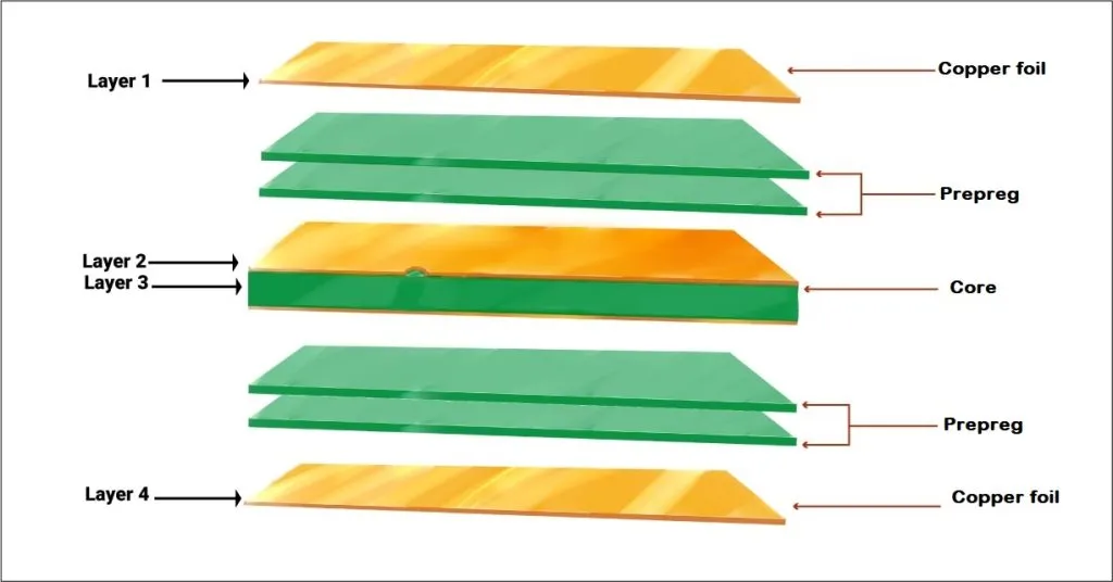
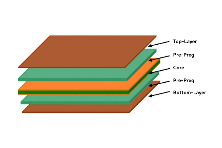
For high-speed designs, always place a ground plane directly next to signal layers. This ensures that return currents follow the shortest path beneath the signal traces, reducing the loop area and minimizing EMI. For instance, in a 4-layer stackup, a common configuration is:
- Layer 1: Signal (Top)
- Layer 2: Ground Plane
- Layer 3: Power Plane
- Layer 4: Signal (Bottom)
This setup keeps the ground plane close to the top signal layer, providing a low-impedance return path. If your design includes multiple signal layers, consider sandwiching them between ground planes in a 6- or 8-layer stackup.
2. Minimize Distance Between Ground and Power Planes
In designs with both power and ground planes, place them close to each other to create a natural capacitance. This capacitance helps filter out high-frequency noise and reduces loop inductance in the power delivery network (PDN). A typical separation of 3 to 5 mils (0.003 to 0.005 inches) between power and ground planes is ideal for most high-speed designs. This tight coupling can lower EMI by stabilizing the power supply and reducing voltage fluctuations.
3. Use Continuous Ground Planes for Quiet Design
A quiet ground plane design means avoiding interruptions or cuts in the ground layer. A continuous, unbroken ground plane provides a consistent return path and minimizes noise. Avoid routing traces through the ground plane or creating large gaps, as these can force return currents to take longer paths, increasing EMI.
For example, in a design operating at 1 GHz, a split or interrupted ground plane can increase crosstalk by 30% or more compared to a solid plane. Keeping the ground plane intact ensures a low-noise environment for your signals.
4. Position Ground Planes to Shield Sensitive Areas
In mixed-signal designs, where analog and digital circuits coexist, ground plane placement can shield sensitive analog components from digital noise. Place the ground plane beneath analog sections to isolate them from high-speed digital signals on other layers. This shielding effect can reduce noise coupling by as much as 15 dB in critical areas.
Signal Integrity and Ground Plane Placement
Signal integrity refers to the quality of electrical signals as they travel through the PCB. Poor signal integrity can lead to data errors, timing issues, and system failures. Ground plane placement plays a crucial role in maintaining signal integrity by providing a stable reference for signals and minimizing impedance mismatches.
Here are key ways ground planes impact signal integrity:
- Controlled Impedance: High-speed signals, such as those in USB 3.0 (5 Gbps) or PCIe (8 GT/s), require controlled impedance to prevent reflections. A ground plane beneath the signal layer helps maintain a consistent impedance, typically around 50 ohms for single-ended traces or 100 ohms for differential pairs.
- Reduced Crosstalk: Placing ground planes between signal layers separates traces and reduces crosstalk. For instance, in a 6-layer stackup, alternating signal and ground layers can cut crosstalk by up to 25% compared to stacked signal layers without shielding.
- Stable Return Paths: Without a nearby ground plane, return currents may take unpredictable paths, leading to signal distortion. A dedicated ground layer ensures return currents flow directly under the signal, preserving signal quality.
Common Split Ground Plane Issues and How to Avoid Them
While ground planes are essential for EMI reduction and signal integrity, splitting them can sometimes cause more problems than solutions. Split ground plane issues arise when the ground layer is divided into separate sections for analog and digital circuits or other purposes. While the intention is often to isolate noise, improper splitting can lead to significant challenges.
Here are some common split ground plane issues and tips to avoid them:
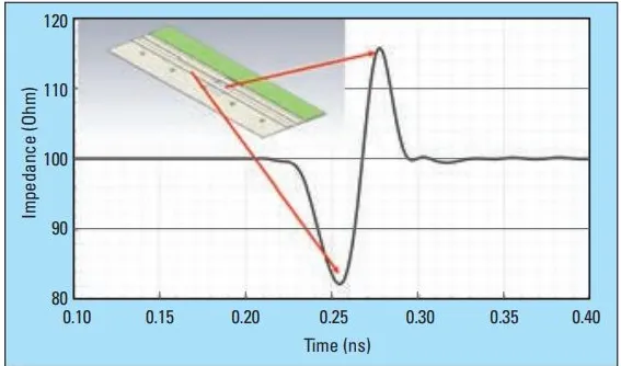
- Return Path Disruptions: Splitting the ground plane can force return currents to take longer paths around the split, creating large loop areas that radiate EMI. To avoid this, ensure splits are minimal and connect the sections with a single-point bridge if necessary.
- Noise Coupling: A split ground plane can allow noise from one section to couple into another, especially if high-speed signals cross the split. Always route high-speed traces away from splits or use a solid ground plane beneath them.
- Impedance Mismatches: Signals crossing a split may experience impedance changes, leading to reflections. If a split is unavoidable, place it away from critical signal paths and use stitching vias to maintain a low-impedance connection across the split.
In many cases, a single, continuous ground plane with careful component placement and routing is a better solution than splitting. If a split is required, simulate the design to predict potential EMI and signal integrity issues before fabrication.
Advanced Tips for Quiet Ground Plane Design
Achieving a quiet ground plane design goes beyond basic placement. Here are advanced strategies to further reduce EMI and enhance performance:
- Use Multiple Ground Planes: In complex designs with 8 or more layers, dedicate multiple layers to ground planes. This provides additional shielding and return paths, especially for high-density boards with mixed signals.
- Stitching Vias: Place vias around the edges of the ground plane to connect it to other ground layers, creating a “cage” effect that traps noise and reduces EMI. Space vias at intervals of about 1/20th of the wavelength of the highest frequency in your design (e.g., 0.15 inches for 1 GHz signals).
- Decoupling Capacitors: Place decoupling capacitors close to IC power pins, connecting them directly to the ground plane. Use values like 0.1 μF for high-frequency noise filtering, ensuring a clean power supply and quieter ground.
Conclusion: Mastering Ground Plane Placement for Low EMI
Optimizing ground plane placement in PCB stackup is a fundamental step toward achieving low EMI and high signal integrity. By placing ground planes adjacent to signal layers, minimizing splits, and following best practices for quiet ground plane design, you can significantly reduce noise and improve the reliability of your designs. Whether you’re working on a simple 4-layer board or a complex multi-layer system, thoughtful ground plane placement can make all the difference.
Remember to consider the specific needs of your design, such as frequency, signal speed, and component placement, when planning your stackup. With the strategies outlined in this guide, you’re well-equipped to tackle EMI challenges and create high-performing PCBs that meet modern standards.
At ALLPCB, we’re committed to supporting your design journey with resources and expertise. Apply these tips in your next project to see the impact of optimized ground plane placement for yourself.


