 ALLPCB


In the fast-paced world of electronics, printed circuit boards (PCBs) are the backbone of countless devices, from smartphones to medical equipment. Ensuring these boards function flawlessly is critical, and that's where In-Circuit Testing (ICT) comes in. ICT is a powerful testing method that verifies the integrity of individual components and connections on a PCB, catching defects early in the manufacturing process. For engineers, understanding ICT is essential to delivering high-quality, reliable products. In this blog, we'll dive into what ICT is, how it works, its benefits, challenges, and best practices, providing actionable insights to enhance your PCB manufacturing process.
What is In-Circuit Testing?
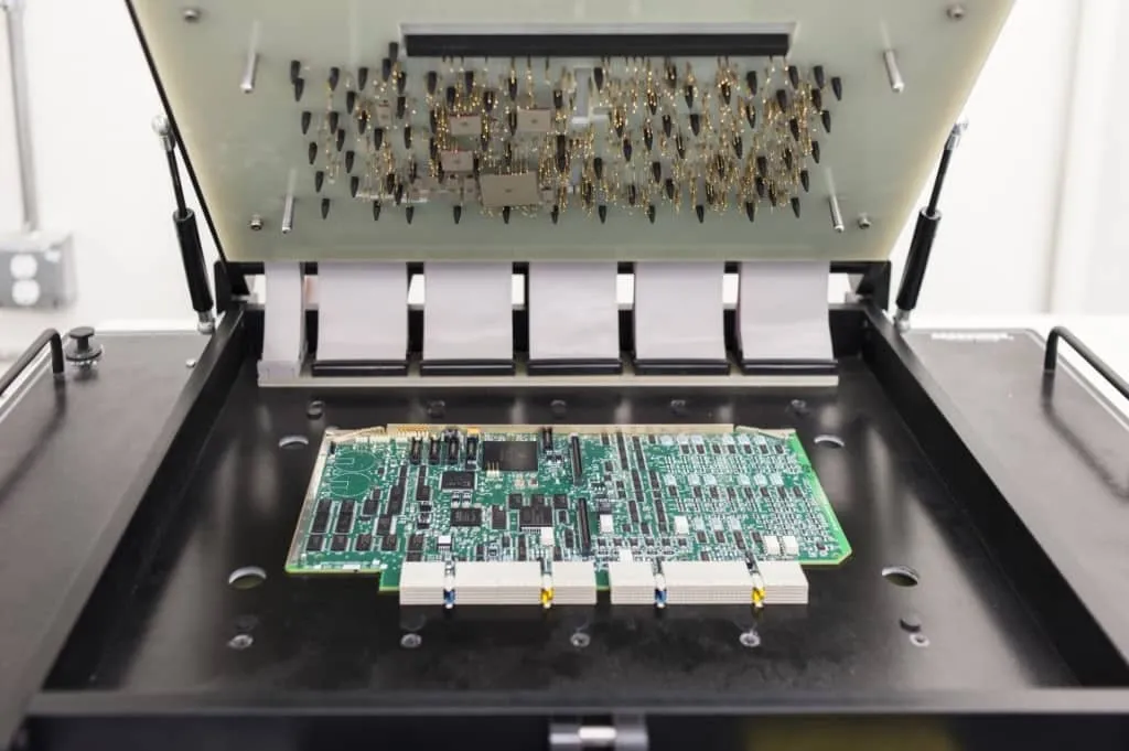
In-Circuit Testing is an automated testing method used during PCB assembly to evaluate the electrical performance of individual components and their connections. Unlike other testing methods that assess overall board functionality, ICT focuses on verifying each component—resistors, capacitors, diodes, and integrated circuits (ICs)—to ensure they meet specified parameters. By using a specialized fixture called a 'bed-of-nails,' ICT applies electrical signals to test points on the PCB, measuring characteristics like resistance, capacitance, and voltage.
ICT is typically performed after the surface-mount technology (SMT) and through-hole components are soldered onto the board but before functional testing. This early-stage testing helps identify manufacturing defects, such as open circuits, short circuits, missing components, or incorrect component values, before they escalate into costly failures.
Why In-Circuit Testing Matters for PCB Manufacturing
The complexity of modern PCBs, with densely packed components and high-speed signals, demands rigorous quality control. A single defective component or solder joint can compromise an entire device, leading to product failures, recalls, or safety hazards. ICT addresses these risks by offering:
- High Fault Coverage: ICT testing can detect up to 98% of manufacturing defects, including shorts, opens, and component failures.
- Early Defect Detection: Identifying issues during assembly reduces rework costs and prevents defective boards from reaching end-users.
- Consistency and Repeatability: Automated ICT systems deliver consistent results, minimizing human error and ensuring reliable testing across high-volume production runs.
For engineers, ICT is a critical tool for meeting stringent industry standards, such as those in automotive, aerospace, and medical sectors, where reliability is non-negotiable.
How In-Circuit Testing Works
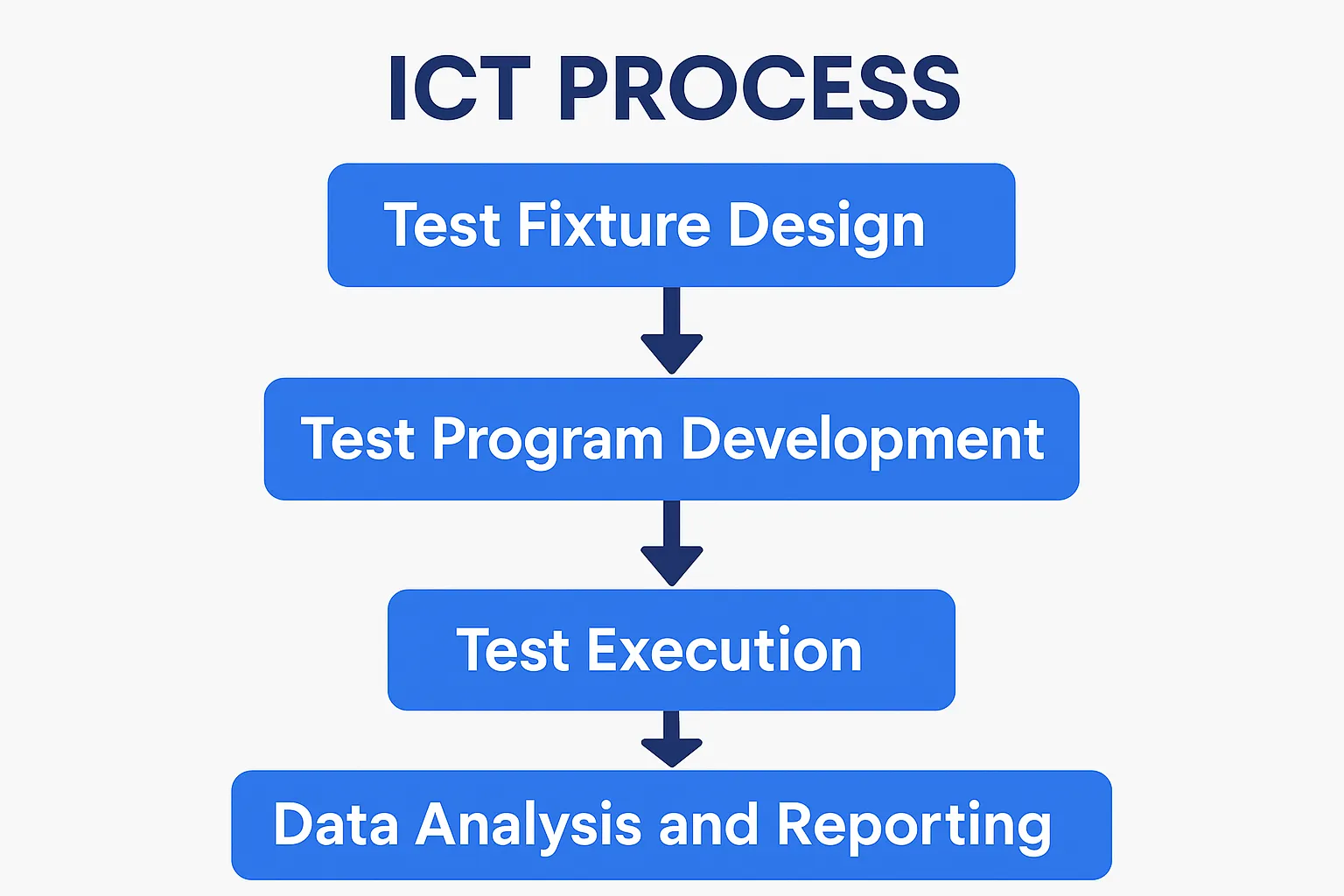
ICT involves a combination of hardware, software, and precise test fixtures tailored to the PCB's design. Here's a step-by-step breakdown of the process:
1. Test Fixture Design
The bed-of-nails fixture is custom-designed for each PCB, with probes aligned to contact specific test points. These probes connect to the ICT system, which generates and measures electrical signals. Fixture design is critical, as poor alignment or inadequate probe contact can lead to inaccurate results.
Suggested Reading: Demystifying ICT Test Fixtures: A Comprehensive Guide for Electronics Engineers
2. Test Program Development
Engineers develop a test program that defines the parameters to be measured, such as resistance (in ohms), capacitance (in farads), or voltage levels. The program also sets pass/fail criteria based on the component's specifications. For example, a resistor rated at 10 kΩ might have a tolerance of ±5%, so the test program checks if its resistance falls between 9.5 kΩ and 10.5 kΩ.
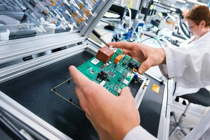
3. Test Execution
The PCB is placed in the fixture, and the ICT system applies electrical signals through the probes. It measures the response of each component and compares it to the expected values. Common measurements include:
- Resistance: Ensuring low resistance for good conductors (e.g., <1 Ω for solder joints).
- Capacitance: Detecting shorts by measuring induced capacity (e.g., <10 pF for adjacent traces).
- Voltage Levels: Verifying correct operation of ICs (e.g., 3.3 V for logic high signals).
- Continuity: Checking for open or short circuits (e.g., no continuity between power and ground).
4. Data Analysis and Reporting
The ICT system generates a report detailing the test results, including any defects and their locations. This precise fault localization enables quick repairs, reducing downtime in the production line.
Benefits of In-Circuit Testing
ICT offers several advantages that make it a cornerstone of PCB manufacturing:
High Accuracy and Speed
ICT systems can test hundreds of components in seconds, making them ideal for high-volume production. Their precision ensures accurate detection of defects, even in complex boards with high-impedance nodes or fine-pitch components. For instance, Keysight's i3070 ICT system minimizes parasitic capacitance and crosstalk, ensuring repeatable measurements.
Cost-Effectiveness for Large Volumes
While the initial setup cost for ICT fixtures (often $10,000–$50,000) is high, the speed and fault coverage make it cost-effective for large production runs. Early defect detection reduces rework costs, which can exceed $100 per board for complex assemblies.
Comprehensive Test Coverage
ICT tests a wide range of components, including resistors, capacitors, diodes, transistors, and ICs. It also verifies solder joint integrity and trace connectivity, ensuring the PCB meets design specifications. This comprehensive coverage is critical for applications like automotive electronics, where failure rates must be below 1 ppm.
Seamless Integration
ICT systems integrate easily into automated production lines, supporting Industry 4.0 standards like IPC-CFX for real-time data exchange. This integration streamlines testing and improves traceability.
Challenges and Limitations of In-Circuit Testing
Despite its strengths, ICT has some limitations that engineers must consider:
High Initial Costs
The custom bed-of-nails fixture and test program development require significant upfront investment. For low-volume or prototype runs, these costs may outweigh the benefits, making alternatives like flying probe testing more suitable.
Design Constraints
ICT requires test points on the PCB, which can increase board size or complexity. For high-density designs with limited space, providing adequate test point access is challenging. Engineers must incorporate Design for Testability (DFT) principles early in the design phase to ensure ICT compatibility.
Measurement Uncertainties
Factors like fixture wiring, probe contact resistance, and component tolerances introduce measurement uncertainties. For example, a resistor with a ±10% tolerance may pass at 9 kΩ but fail at 8.9 kΩ, depending on the test setup. Careful calibration and tolerance analysis are essential to minimize false failures.
Limited Functional Testing
ICT focuses on component-level testing and does not verify the PCB's overall functionality. For example, it can confirm a capacitor's value but not whether the circuit performs as intended. Functional testing (FCT) is often needed to complement ICT.
Best Practices for Effective In-Circuit Testing
To maximize the benefits of ICT, engineers should follow these best practices:
Incorporate Design for Testability (DFT)
Design PCBs with ICT in mind by including accessible test points for critical nodes. Aim for test point diameters of at least 0.035 inches and spacing of 0.1 inches to ensure reliable probe contact. Use DFT analysis tools, like Keysight's x1149, to optimize test coverage.
Optimize Test Fixture Design
Work closely with fixture designers to ensure precise probe alignment and minimal signal interference. Use high-quality probes with low contact resistance (e.g., <50 mΩ) to improve measurement accuracy.
Calibrate and Validate Test Programs
Regularly calibrate ICT systems to account for environmental factors like temperature and humidity, which can affect measurements. Validate test programs against known-good boards to establish baseline performance.
Combine ICT with Other Testing Methods
Pair ICT with functional testing and automated optical inspection (AOI) for comprehensive quality control. For example, AOI can detect visual defects like solder bridges, while ICT verifies electrical performance, and FCT ensures system-level functionality.
Analyze and Act on Test Data
Use ICT reports to identify recurring defects and improve manufacturing processes. For instance, if multiple boards fail due to solder joint issues, adjust the reflow oven profile to achieve a peak temperature of 245°C for lead-free solder.
ALLPCB's Role in Supporting ICT and PCB Quality
At ALLPCB, we understand the importance of rigorous testing to deliver reliable PCBs. Our advanced manufacturing facilities and quick-turn prototyping services enable engineers to iterate designs rapidly, incorporating DFT principles for seamless ICT integration. With global logistics and a commitment to quality, we provide high-quality PCB assemblies that meet the demands of ICT, ensuring your boards are tested and ready for production. Whether you're developing automotive electronics or IoT devices, ALLPCB's expertise supports your journey from design to market.
Conclusion
In-Circuit Testing is a vital tool for ensuring the quality and reliability of PCBs in today's complex electronics landscape. By detecting defects early, ICT saves time, reduces costs, and enhances product performance. While challenges like high setup costs and design constraints exist, following best practices like DFT and combining ICT with other testing methods can overcome these hurdles. For engineers, mastering ICT is key to delivering robust, high-quality PCBs that power the devices we rely on daily. At ALLPCB, we're here to support your testing and manufacturing needs, helping you bring innovative products to market with confidence.


