 ALLPCB


Are you looking to turn your electronic ideas into a working printed circuit board (PCB)? The PCB prototype manufacturing process can seem complex, but with the right guidance, it’s a manageable journey from design to reality. Whether you're an engineer, hobbyist, or startup founder, this guide will walk you through every stage, from creating your design with PCB design software to generating Gerber files, following PCB fabrication steps, and completing the PCB assembly process. Let’s dive into the detailed steps to help you build a successful PCB prototype with precision and ease.
What Is PCB Prototype Manufacturing?
PCB prototype manufacturing is the process of creating a small batch of printed circuit boards to test and validate a design before mass production. It’s a crucial step in electronics development, allowing you to identify errors, refine functionality, and ensure your product meets performance standards. The process involves designing the circuit, fabricating the board, and assembling components. By following a structured approach, you can save time, reduce costs, and achieve a reliable final product.
Why PCB Prototyping Matters
Prototyping is essential for catching design flaws early. A single error in trace placement or component selection can lead to signal interference or thermal issues, costing thousands of dollars in rework during mass production. For instance, a poorly designed power trace might result in impedance mismatches, affecting signal speeds by up to 30% in high-frequency applications. Testing a prototype helps you avoid such pitfalls, ensuring your design is ready for larger-scale manufacturing.
Step 1: Designing Your PCB with the Right Software
The first step in the PCB prototype manufacturing process is creating a digital design using PCB design software. This tool allows you to draw schematics, place components, and route traces. Popular software options include programs that offer user-friendly interfaces and advanced features for both beginners and professionals. When choosing software, look for features like schematic capture, layout editing, and 3D visualization to ensure accuracy.
Start by sketching your circuit schematic, which acts as a blueprint for electrical connections. Then, move to the layout phase, where you arrange components on a virtual board. Pay attention to trace widths (e.g., 0.2 mm for low-current signals) and spacing to prevent crosstalk, especially in high-speed designs operating at frequencies above 100 MHz. Proper design at this stage minimizes errors during fabrication.
Tips for Effective PCB Design
- Keep power and ground planes close to reduce electromagnetic interference (EMI).
- Use design rule checks (DRC) to catch errors like overlapping traces or incorrect clearances.
- Simulate your design to predict performance under real-world conditions.
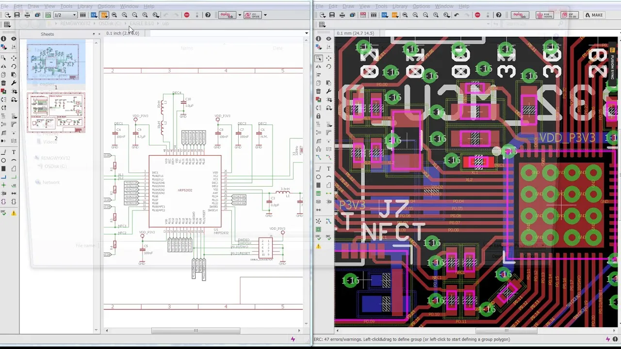
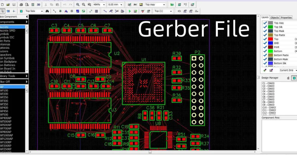
Step 2: Gerber File Generation for Manufacturing
Once your design is complete, the next step is Gerber file generation. Gerber files are the industry-standard format used by manufacturers to interpret your PCB design. These files contain detailed instructions for each layer of the board, including copper traces, solder masks, and drill holes. Most PCB design software includes a built-in tool to export Gerber files, ensuring compatibility with fabrication equipment.
To generate Gerber files, select the export option in your software and choose the layers to include, such as top copper, bottom copper, and silkscreen. Double-check the output for errors—missing layers or incorrect scaling can lead to fabrication delays. For example, a drill file (often in Excellon format) must align perfectly with the board dimensions, or holes might be misplaced by as much as 0.1 mm, causing component fit issues.
Best Practices for Gerber File Generation
- Include a readme file with your Gerber set to explain layer functions to the manufacturer.
- Verify file extensions (e.g., .GTL for top layer, .GBL for bottom layer) match industry standards.
- Review the files in a Gerber viewer to spot errors before submission.
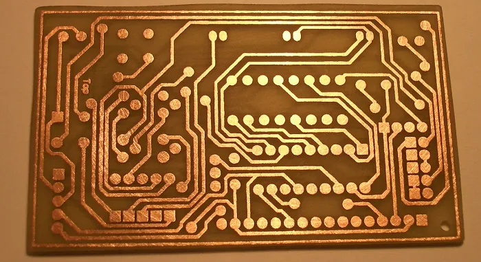
Step 3: PCB Fabrication Steps – Turning Files into Boards
With your Gerber files ready, it’s time for the PCB fabrication steps. This process transforms your digital design into a physical board through a series of precise manufacturing stages. Understanding these steps helps you prepare a design that’s easy to fabricate and meets quality standards.
Key PCB Fabrication Steps
- Design Verification: The manufacturer reviews your files for errors, ensuring traces meet minimum spacing (e.g., 6 mils for standard boards) and drill sizes are feasible.
- Material Preparation: A substrate like FR-4, with a dielectric constant of around 4.5, is selected and layered with copper foil.
- Imaging and Etching: Your design is transferred to the copper using a photoresist process, and unwanted copper is etched away to form traces.
- Drilling: Holes for vias and components are drilled with precision, often to tolerances of ±0.05 mm.
- Plating: Copper is plated onto drilled holes to create electrical connections between layers.
- Solder Mask and Silkscreen: A protective solder mask is applied, and a silkscreen layer adds labels for components.
- Testing: Boards undergo electrical tests to check for shorts or opens, ensuring functionality before shipment.
Choosing a reliable manufacturing partner is critical during fabrication. Look for providers with strict quality control and the ability to handle specific requirements, such as multilayer boards or fine-pitch designs.
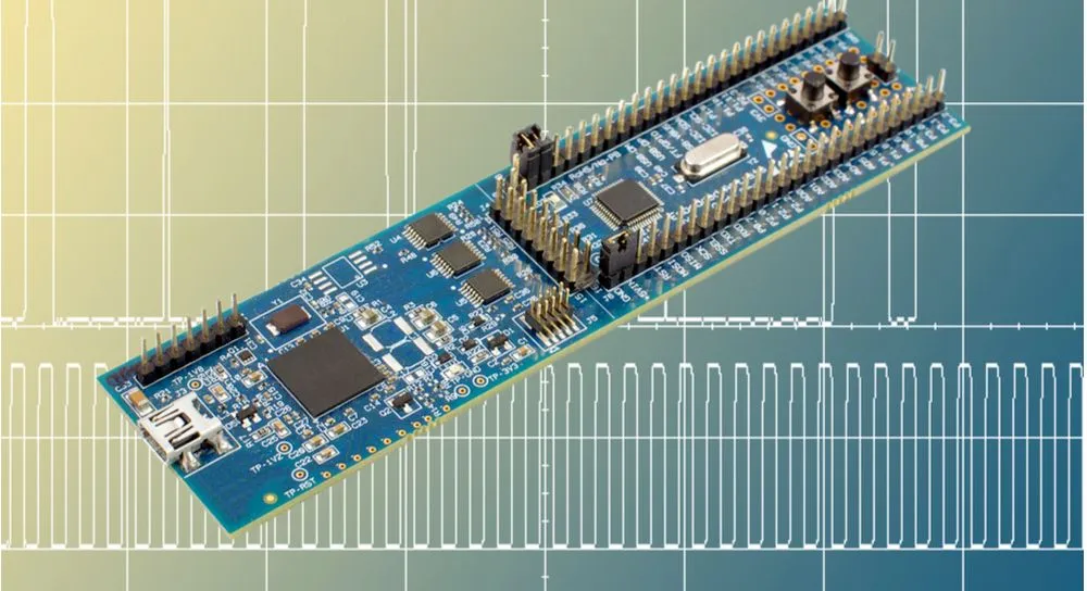
Step 4: PCB Assembly Guide – Bringing Your Board to Life
After fabrication, the PCB assembly process begins. This stage involves placing and soldering components onto the board to create a functional circuit. Assembly can be done manually for small prototypes or through automated processes like surface-mount technology (SMT) for larger batches.
Steps in PCB Assembly
- Bill of Materials (BOM) Preparation: Create a detailed BOM listing all components, including part numbers, quantities, and specifications (e.g., a 10 kΩ resistor with 1% tolerance).
- Stencil Creation: A stencil is used to apply solder paste precisely to pads where components will be placed.
- Component Placement: Components are placed on the board, either by hand or using pick-and-place machines for accuracy within 0.02 mm.
- Reflow Soldering: The board passes through a reflow oven, melting solder paste at temperatures up to 250°C to secure components.
- Inspection: Automated optical inspection (AOI) checks for misaligned components or soldering defects.
- Functional Testing: The assembled board is powered on to verify it operates as designed, measuring parameters like voltage levels or signal integrity.
Pay attention to thermal profiles during reflow soldering to prevent component damage. For instance, exceeding 260°C for lead-free solder can degrade sensitive ICs, reducing lifespan by up to 20%. Clear communication with your assembly provider ensures they follow your specifications.
Step 5: Testing and Iteration for Perfection
Testing is the final step in the PCB prototype manufacturing process. Even with careful design and assembly, issues like signal noise or thermal hotspots can arise. Use tools like oscilloscopes to measure signal speeds (e.g., ensuring rise times below 1 ns for high-speed signals) and thermal cameras to detect temperature variations above 10°C across the board.
If problems are found, iterate on your design. Update your schematic or layout, regenerate Gerber files, and produce a new prototype. Each iteration brings you closer to a flawless design ready for mass production. Document every change to track improvements and avoid repeating mistakes.
Common Challenges in PCB Prototyping and How to Overcome Them
The road to a successful PCB prototype isn’t always smooth. Here are some common hurdles and solutions:
- Design Errors: Missed connections or incorrect footprints can halt progress. Always run DRC and simulate your design before fabrication.
- Thermal Issues: Uneven heat distribution can cause failures. Use copper pours and vias to dissipate heat evenly, targeting a temperature uniformity within 5°C.
- Component Sourcing Delays: Unavailable parts can delay assembly. Maintain a flexible BOM with alternative components to avoid bottlenecks.
How ALLPCB Supports Your PCB Prototype Journey
At ALLPCB, we’re committed to making your PCB prototype manufacturing process seamless. Our services cover every step, from design review to fabrication and assembly. We offer quick turnaround times, ensuring your prototype is ready for testing in days, not weeks. With strict quality checks, like automated optical inspection and electrical testing, we guarantee boards that meet your specifications. Whether you need a single-layer board or a complex multilayer design, our team is here to help you succeed.
Conclusion: Turning Ideas into Working Prototypes
Creating a PCB prototype is a rewarding process that bridges the gap between concept and reality. By following this step-by-step guide, you can navigate the PCB prototype manufacturing process with confidence. From designing with powerful PCB design software to mastering Gerber file generation, executing precise PCB fabrication steps, and following a detailed PCB assembly guide, each stage builds toward a functional product. Start small, test thoroughly, and iterate as needed to perfect your design. With the right approach and support from ALLPCB, your electronic innovations are just a prototype away from making an impact.


