ALLPCB


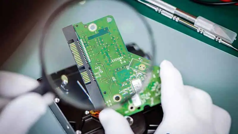
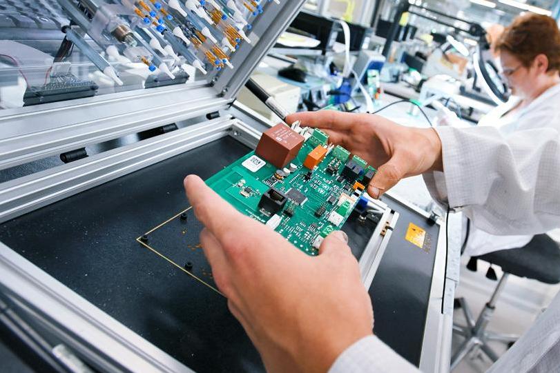
If you're an electronics engineer looking to understand ICT test fixture basics or wondering what is ICT testing, you're in the right place. In-Circuit Testing (ICT) is a crucial method used in electronics manufacturing to check the functionality of individual components on a printed circuit board (PCB) without powering up the entire system. An ICT test fixture is a custom tool designed to hold the PCB and connect it to a tester for accurate measurements. In this guide, we'll break down in-circuit testing explained, dive into ICT fixture components, and walk through the ICT fixture process to help you master this essential testing technique.
Whether you're designing PCBs or managing production, understanding ICT can save time, reduce costs, and ensure quality. Let’s explore everything you need to know in a clear, step-by-step way.
What Is ICT Testing? A Simple Overview for Engineers
What is ICT testing? At its core, ICT, or In-Circuit Testing, is a method used to test individual components on a PCB while they are still in the circuit. Unlike functional testing, which checks the overall operation of a board, ICT focuses on verifying specific parameters like resistance, capacitance, and continuity. It’s typically done before the final assembly to catch defects early.
ICT is widely used in high-volume manufacturing because it’s fast and automated. For instance, an ICT system can test hundreds of points on a PCB in just a few seconds, ensuring that resistors are within their specified range (e.g., ±5% tolerance) or that capacitors meet their rated values (e.g., 10 μF). This precision helps engineers avoid costly rework later in production.
Why does this matter to you? As an electronics engineer, PCB in circuit test gives you confidence that each component works as intended before the board moves to the next stage. It’s a proactive way to maintain quality control.
In-Circuit Testing Explained: How It Works
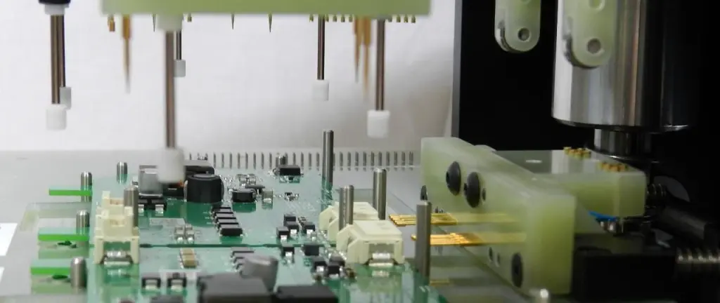
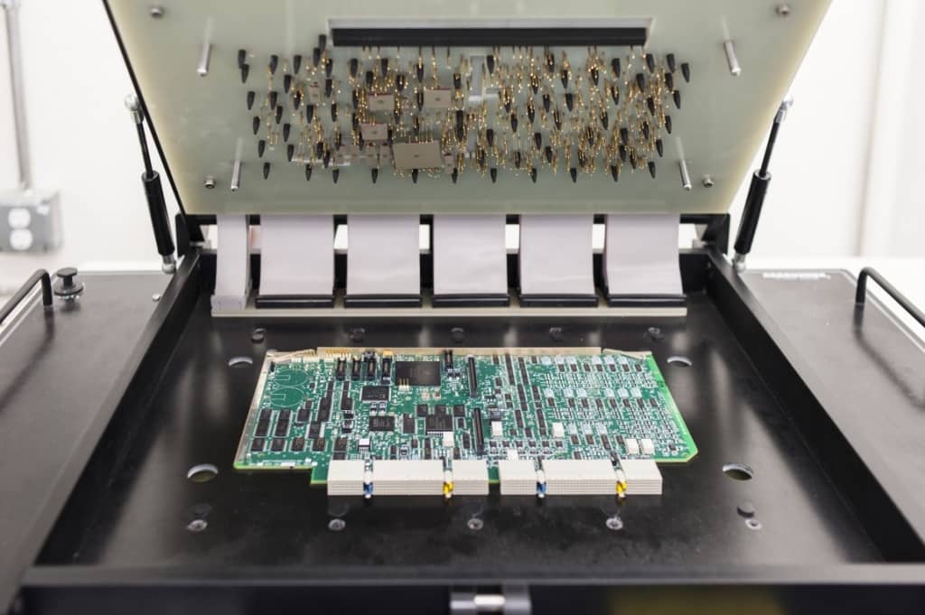
Let’s dive deeper into in-circuit testing explained. ICT works by using a specialized tester connected to the PCB through a fixture. The fixture, often called a "bed of nails," has multiple spring-loaded probes that make contact with specific test points on the board. These probes send electrical signals to measure values like voltage, current, or resistance at each point.
Here’s a basic rundown of how ICT operates:
- Setup: The PCB is placed in the ICT fixture, aligning test points with the probes.
- Connection: The fixture connects the PCB to the ICT machine, which is programmed with the board’s design data.
- Testing: The machine sends signals through the probes to test components. For example, it might check if a resistor measures 1 kΩ as specified or detect an open circuit where continuity is expected.
- Results: The system logs pass/fail results for each test point, often flagging issues like a short circuit or a misplaced component.
ICT is highly effective for detecting manufacturing defects. According to industry data, ICT can catch up to 85-90% of assembly faults, such as solder bridges or incorrect component values, before they cause bigger problems.
For engineers, understanding this process means you can design boards with ICT in mind—placing test points strategically to ensure full coverage. This foresight can reduce test times and improve accuracy.
ICT Test Fixture Basics: What You Need to Know
Now, let’s cover ICT test fixture basics. An ICT test fixture is a custom-made device that holds the PCB securely and provides electrical connections between the board and the ICT tester. Think of it as a bridge that allows the tester to "talk" to the PCB.
Fixtures are tailored to each PCB design because every board has unique test points and layouts. Building a fixture can take time and cost anywhere from $1,000 to $10,000 depending on complexity, but it’s a worthwhile investment for high-volume production. For low-volume or prototype runs, some engineers opt for flying probe testers, which don’t require a fixture but are slower.
Why are fixtures so important? Without a properly designed fixture, you risk poor contact between probes and test points, leading to false failures or missed defects. A good fixture ensures repeatable, reliable results—crucial for maintaining production quality.
ICT Fixture Components: Breaking Down the Essentials
Understanding ICT fixture components is key to designing or using one effectively. Here are the main parts of a typical ICT fixture and their roles:
- Base Plate: This is the foundation of the fixture, usually made of durable materials like aluminum or high-grade plastic. It holds all other components and ensures stability during testing.
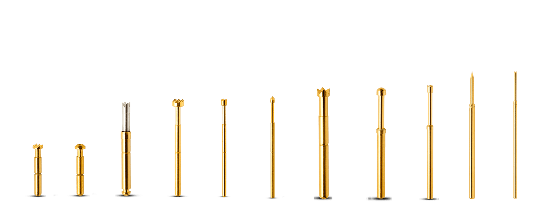
- Probe Plate: This plate contains hundreds or even thousands of spring-loaded probes (pogo pins) that contact the PCB’s test points. Probes are often rated for specific currents, like 2-3 amps, to handle various signals without damage.
- Alignment Pins: These pins ensure the PCB is positioned correctly on the fixture, preventing misalignment that could lead to inaccurate tests.
- Pressure Mechanism: A clamping system or pneumatic press applies even pressure to hold the PCB against the probes, ensuring consistent contact. Pressure might range from 5 to 10 psi depending on the design.
- Wiring and Interface: Wires connect the probes to the ICT tester, often through a standardized interface like a D-sub connector. This setup transfers signals for analysis.
Each component must be precise. For example, if probes are misaligned by even 0.1 mm, they might miss a test pad, causing a false reading. As an engineer, you’ll work with fixture designers to specify probe locations based on your PCB layout, often using CAD files for accuracy.
Suggested Reading: ICT Test Fixture Maintenance: Extending Lifespan and Ensuring Reliability
The ICT Fixture Process: Step-by-Step for Electronics Engineers
Let’s walk through the ICT fixture process so you can see how it fits into PCB testing and manufacturing. This step-by-step guide will help you prepare for or oversee ICT in your projects.
Step 1: Design for Testability (DFT)
Before a fixture is even built, you need to design your PCB with ICT in mind. This means adding test points—small pads or vias—where probes can make contact. For example, place test points near critical components like ICs or high-value resistors (e.g., 10 kΩ) to verify their values. Industry standards suggest a minimum test point size of 1 mm for reliable contact.
Step 2: Fixture Design and Fabrication
Once your PCB design is finalized, the fixture is designed using data from your Gerber files or CAD layout. Engineers specify probe locations, and the fixture is built to match. This process can take 2-4 weeks for complex boards. Costs vary, but a typical fixture for a medium-sized PCB might run around $3,000.
Step 3: Fixture Validation
Before mass testing, the fixture is validated with a sample PCB. Engineers check for proper alignment and contact, adjusting probes if needed. A common issue is insufficient probe pressure, which might require tweaking the clamping force to, say, 8 psi for better results.
Step 4: Programming the ICT Tester
The ICT machine is programmed with test parameters based on your board’s bill of materials (BOM) and schematic. For instance, if a capacitor should be 22 μF, the tester is set to flag any value outside a ±10% tolerance. This step ensures the tester knows what to look for.
Step 5: Testing and Analysis
With the fixture ready, PCBs are loaded and tested. A typical ICT run might check 500 test points in under 10 seconds, measuring parameters like resistance down to 0.1 ohms for accuracy. Results are logged, and failed boards are flagged for rework.
Step 6: Maintenance and Iteration
Fixtures require regular maintenance as probes wear out after thousands of cycles—often around 50,000 contacts. Worn probes can cause false readings, so they’re replaced periodically. If your PCB design changes, the fixture may need updates, which can cost extra time and money.
By following this process, you can integrate ICT into your workflow, catching defects early and ensuring your boards meet specs. For example, I’ve seen projects where ICT reduced defect rates by 30% in the first month of implementation, saving thousands in rework costs.
Benefits and Challenges of ICT Testing for Engineers
ICT offers clear advantages, but it’s not without hurdles. Here’s a balanced look to help you decide if it’s right for your project.
Benefits
- Early Defect Detection: ICT catches issues like shorts or wrong components before final assembly, reducing rework costs by up to 40% in some cases.
- Speed: Automated testing means hundreds of points are checked in seconds, ideal for high-volume runs of 10,000+ units.
- Accuracy: ICT provides precise measurements, often within 0.01% of expected values, ensuring reliability.
Challenges
- High Initial Cost: Fixtures and ICT systems can cost $50,000 or more upfront, a barrier for small-scale projects.
- Design Constraints: Adding test points takes up board space, which can be tricky for compact designs like wearable tech.
- Fixture Updates: If your PCB layout changes, the fixture must be modified, adding delays of 1-2 weeks.
For engineers, weighing these factors is key. If you’re working on a high-volume product like a consumer gadget, ICT is often worth the investment. For prototypes, consider alternatives like flying probe testing to avoid fixture costs.
Tips for Optimizing ICT in Your Workflow
Here are practical tips to make ICT work better for you as an electronics engineer:
- Plan Test Points Early: During schematic design, allocate space for test points near high-risk components. Aim for at least one test point per net for full coverage.
- Collaborate on Fixture Design: Work closely with fixture manufacturers to ensure probes match your board’s pad sizes—typically 1-1.5 mm for standard designs.
- Use Simulation Tools: Software like Altium or Cadence can simulate ICT coverage, helping you spot untested areas before fabrication.
- Monitor Fixture Wear: Track probe life cycles and replace them after 40,000-50,000 uses to avoid false negatives.
These steps can streamline your testing process, saving hours during production. In one project I supported, optimizing test point placement cut ICT setup time by 25%, speeding up the entire testing phase.
Conclusion: Mastering ICT Test Fixtures for Better Electronics Design
ICT test fixtures and in-circuit testing are powerful tools for electronics engineers aiming to ensure quality and efficiency in PCB manufacturing. From understanding what is ICT testing to mastering the ICT fixture process, this guide has covered the essentials—ICT test fixture basics, in-circuit testing explained, and ICT fixture components. By integrating ICT into your workflow, you can catch defects early, reduce costs, and deliver reliable products.