 ALLPCB


When designing printed circuit boards (PCBs), one of the critical factors that engineers must consider is the minimum drill size for vias. But why does this matter? Simply put, the drill size of PCB vias directly impacts signal integrity, especially in high-speed designs. Smaller via drill sizes can affect impedance, while larger ones may introduce unwanted signal reflections due to stub lengths. In this comprehensive guide, we'll break down the relationship between PCB via drill size, impedance, and signal integrity, focusing on key aspects like minimum via drill size for high-speed design, microvia drill size, and backdrilling via stub length.
Whether you're working on a high-speed digital circuit or a compact design with microvias, understanding how via drill size influences performance is essential. Let’s dive into the details to help you make informed decisions for your next project.
Why PCB Via Drill Size Matters for Signal Integrity
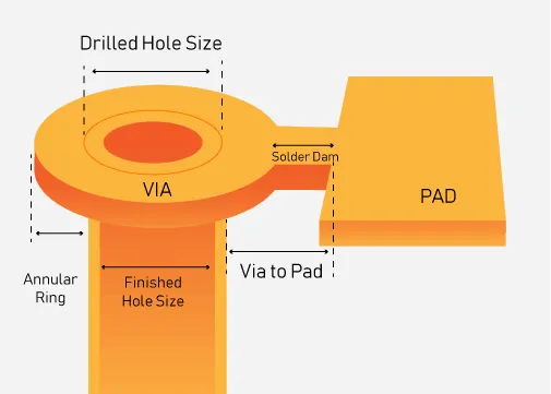
Vias are the tiny holes in a PCB that connect different layers of the board, allowing signals to pass through. The size of these holes, determined by the drill size, plays a significant role in how signals behave. In high-speed designs, where signals can operate at frequencies above 1 GHz, even small variations in via size can lead to impedance mismatches, signal reflections, and loss of data integrity.
For instance, a via with a larger drill size might create a longer stub (the unused portion of the via), which acts like an antenna, causing signal distortions. On the other hand, a smaller drill size can increase capacitance and alter the impedance of the signal path. Balancing these factors is crucial, especially when dealing with high-speed signals where timing and clarity are everything.
Understanding PCB Via Drill Size and Impedance
Impedance is the measure of opposition a circuit presents to a signal. In PCB design, maintaining consistent impedance along a signal path is vital for minimizing signal loss and reflections. The drill size of a via directly influences this impedance. A larger via drill size typically results in lower inductance but may increase capacitance, while a smaller via drill size can do the opposite.
For example, in a high-speed design operating at 5 GHz, a via with a drill size of 0.3 mm might introduce a capacitance of around 0.2 pF, altering the impedance from the ideal 50 ohms to something higher or lower, depending on the stackup. This mismatch can cause signal reflections, leading to data errors. To mitigate this, engineers often use simulation tools to model the impact of via drill size on impedance and adjust their designs accordingly.
One rule of thumb is to keep the via drill size as small as possible without compromising manufacturability. Most modern fabrication processes can handle drill sizes down to 0.15 mm for standard vias, though this depends on the PCB thickness and aspect ratio (the ratio of via depth to diameter). Smaller sizes help maintain tighter control over impedance, which is critical for high-speed designs.
Minimum Via Drill Size in High-Speed Design
In high-speed PCB design, the minimum via drill size becomes even more critical. Signals traveling at high frequencies are extremely sensitive to any disruptions in their path. A via that’s too large can create a stub effect, where the unused portion of the via resonates at certain frequencies, causing signal loss. Conversely, a via that’s too small may not be manufacturable or could increase parasitic capacitance, again affecting signal integrity.
For high-speed designs, a minimum via drill size of 0.2 mm to 0.3 mm is often recommended for through-hole vias, though this can vary based on the specific requirements of the design and the capabilities of the fabrication house. This size range strikes a balance between maintaining signal integrity and ensuring the vias can be reliably drilled and plated.
In designs operating at 10 Gbps or higher, engineers often turn to techniques like backdrilling to remove via stubs or opt for microvias with even smaller drill sizes. These strategies help minimize the impact of vias on signal performance, ensuring cleaner data transmission.
Microvia Drill Size: Precision for High-Density Designs
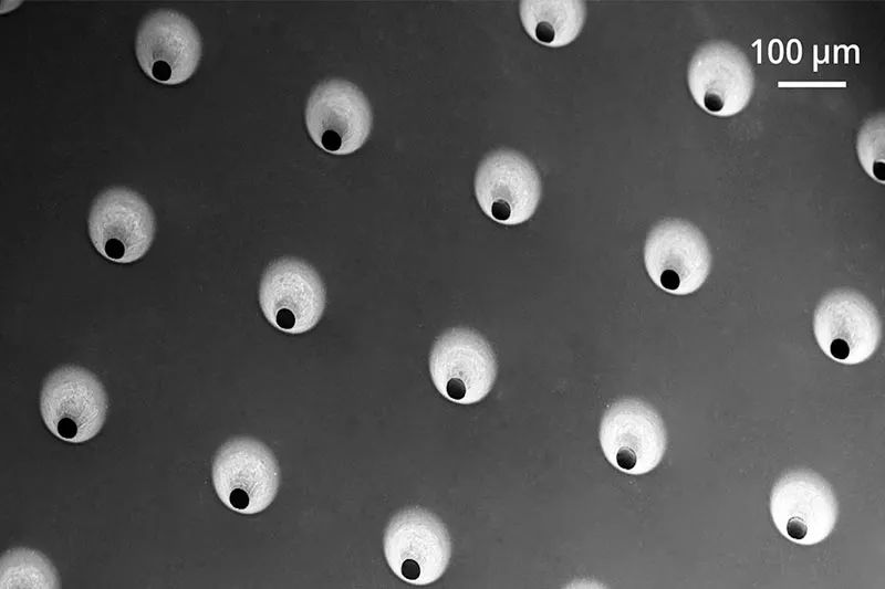
Microvias are a game-changer in high-density interconnect (HDI) designs, where space is at a premium. These vias are much smaller than traditional through-hole vias, often with drill sizes ranging from 0.1 mm to 0.15 mm. They are typically used to connect only a few layers of the PCB, reducing the stub length and minimizing signal integrity issues.
The smaller microvia drill size offers several advantages in high-speed and high-density designs. First, it reduces parasitic capacitance and inductance, helping to maintain consistent impedance. Second, it allows for tighter routing, which is essential in compact devices like smartphones or IoT modules. However, working with such small drill sizes comes with challenges, including higher manufacturing costs and the need for advanced drilling technologies like laser drilling.
Laser-drilled microvias, for instance, can achieve drill sizes as small as 0.075 mm, but they require precise control to avoid defects like incomplete plating or misalignment. When designing with microvias, it’s important to collaborate closely with your fabrication partner to ensure the chosen drill size is within their capabilities and meets the reliability requirements of your project.
Backdrilling and Via Stub Length: A Solution for Signal Integrity
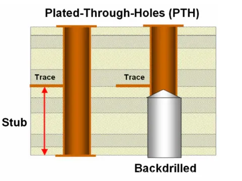
In high-speed designs, one of the biggest challenges with through-hole vias is the stub length—the unused portion of the via that extends beyond the signal path. This stub can act as a resonant structure, causing signal reflections and degrading performance. For signals operating at 5 Gbps or higher, even a stub length of 1 mm can introduce significant noise.
Backdrilling is a manufacturing technique used to address this issue. It involves drilling a larger hole from the opposite side of the PCB to remove the unused copper barrel of the via, effectively shortening the stub length. By reducing the stub to less than 0.25 mm, backdrilling can significantly improve signal integrity, especially for frequencies above 2 GHz.
For example, in a 12-layer PCB where a signal transitions from layer 1 to layer 3, the via stub might extend down to layer 12, creating a long resonant path. After backdrilling, the stub is reduced, and simulations often show a reduction in signal loss by up to 30%. However, backdrilling adds cost and complexity to the manufacturing process, so it’s typically reserved for critical high-speed applications.
When considering backdrilling, the original via drill size still matters. A smaller drill size (e.g., 0.25 mm) paired with backdrilling can offer the best of both worlds—minimal stub effects and controlled impedance. Engineers must weigh the benefits against the added cost to decide if this technique is necessary for their design.
Factors to Consider When Choosing Minimum Via Drill Size
Selecting the right minimum via drill size for your PCB design involves balancing several factors. Here are the key considerations to keep in mind:
- Signal Speed: Higher frequencies require smaller via drill sizes or techniques like backdrilling to minimize stub effects and maintain signal integrity. For designs above 5 Gbps, aim for drill sizes below 0.3 mm if possible.
- Board Thickness: Thicker boards have a higher aspect ratio (via depth to diameter), which can limit the minimum drill size. For boards thicker than 2 mm, drill sizes below 0.2 mm may be challenging to manufacture reliably.
- Manufacturing Capabilities: Not all fabrication houses can handle extremely small drill sizes or advanced techniques like laser drilling for microvias. Always confirm the capabilities and tolerances of your manufacturer before finalizing your design.
- Cost: Smaller drill sizes and advanced processes like backdrilling or microvia fabrication increase production costs. Balance performance needs with budget constraints.
- Impedance Requirements: Use simulation tools to model how via drill size affects impedance. Aim for sizes that keep impedance close to the target value (e.g., 50 ohms for most high-speed signals).
By carefully evaluating these factors, you can choose a via drill size that optimizes both signal integrity and manufacturability for your specific application.
Practical Tips for Optimizing Via Drill Size in Your Design
Now that we’ve covered the theory behind PCB via drill size and signal integrity, let’s look at some practical steps you can take to optimize your designs:
- Use Simulation Tools: Software like signal integrity simulators can help predict how different via drill sizes affect impedance and signal performance. Run simulations early in the design process to identify potential issues.
- Minimize Via Stubs: Route signals to avoid long via stubs. If stubs are unavoidable, consider backdrilling for high-speed signals above 2 GHz.
- Opt for Microvias in HDI Designs: For compact, high-density boards, microvias with drill sizes of 0.1 mm to 0.15 mm can save space and improve signal integrity.
- Collaborate with Your Manufacturer: Discuss minimum drill size capabilities and tolerances with your fabrication partner to ensure your design is manufacturable without compromising performance.
- Test and Validate: After fabrication, test your PCB for signal integrity using tools like time-domain reflectometry (TDR) to measure impedance and identify any mismatches caused by via drill sizes.
Following these tips can help you achieve a design that performs reliably, even under the demanding conditions of high-speed applications.
Conclusion: Striking the Right Balance with Via Drill Size
The minimum drill size for PCB vias is more than just a manufacturing detail—it’s a critical factor in ensuring signal integrity, especially in high-speed and high-density designs. Whether you’re dealing with standard through-hole vias, microvias, or advanced techniques like backdrilling, understanding the relationship between via drill size, impedance, and stub length is key to optimizing your PCB’s performance.
By choosing the right via drill size—often in the range of 0.2 mm to 0.3 mm for high-speed designs—and leveraging techniques like backdrilling for stub reduction, you can minimize signal loss and maintain consistent impedance. For compact HDI designs, microvias with drill sizes as small as 0.1 mm offer a powerful solution, though they require careful planning and coordination with your manufacturer.
Ultimately, the goal is to balance performance, cost, and manufacturability. With the insights and tips provided in this guide, you’re well-equipped to make informed decisions about via drill sizes in your next PCB project, ensuring robust signal integrity and reliable operation.


