 ALLPCB


When it comes to designing a printed circuit board (PCB), every detail matters. One often overlooked factor that plays a critical role in ensuring a board's performance and longevity is the via aspect ratio. If you're searching for ways to improve PCB via reliability, understand via aspect ratio calculation, tackle high aspect ratio via problems, or address via plating issues, you're in the right place. In this comprehensive guide, we'll dive deep into why via aspect ratio is a cornerstone of reliable PCB design and how mastering it can save you from costly failures.
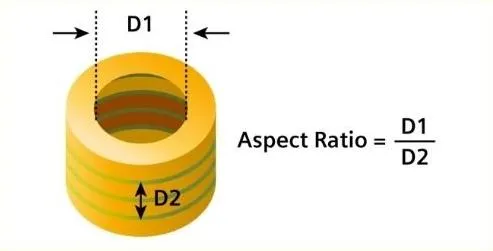
At its core, via aspect ratio is the relationship between the thickness of a PCB and the diameter of the drilled hole for a via. Getting this ratio right ensures proper plating, structural integrity, and electrical performance. In the sections below, we'll explore the ins and outs of this concept, breaking down complex ideas into simple, actionable insights for engineers and designers.
What Is Via Aspect Ratio and Why Does It Matter?
Via aspect ratio is defined as the ratio of a PCB's thickness to the diameter of a via's drilled hole. For example, if a board is 1.6 mm thick and the via hole diameter is 0.2 mm, the aspect ratio is 8:1. This number is crucial because it directly impacts how well a via can be plated with copper during manufacturing. A poorly plated via can lead to weak connections, signal loss, or even complete board failure.
Why does this matter for PCB via reliability? Vias are the tiny pathways that connect different layers of a PCB, carrying electrical signals or power between them. If the aspect ratio is too high—meaning the hole is too narrow compared to the board's thickness—it becomes difficult for plating solutions to reach deep into the via. This can result in uneven or incomplete copper deposition, leading to cracks, voids, or weak spots that compromise the board's performance.
In short, a balanced via aspect ratio ensures that vias are strong, conductive, and reliable, even under thermal stress or high-frequency conditions. Let's break down how to calculate this ratio and what it means for your design.
How to Perform Via Aspect Ratio Calculation
Calculating the via aspect ratio is a straightforward process, but it requires precision to ensure your design meets manufacturing capabilities. Here's the step-by-step method for via aspect ratio calculation:
- Measure the PCB Thickness: Determine the total thickness of your PCB. For a standard four-layer board, this might be around 1.6 mm.
- Measure the Via Hole Diameter: Identify the diameter of the drilled hole for your via. For through-hole vias, this could range from 0.2 mm to 0.5 mm, depending on your design.
- Divide Thickness by Diameter: Divide the PCB thickness by the via diameter to get the aspect ratio. For a 1.6 mm thick board with a 0.3 mm via hole, the calculation is 1.6 / 0.3 = 5.33:1.
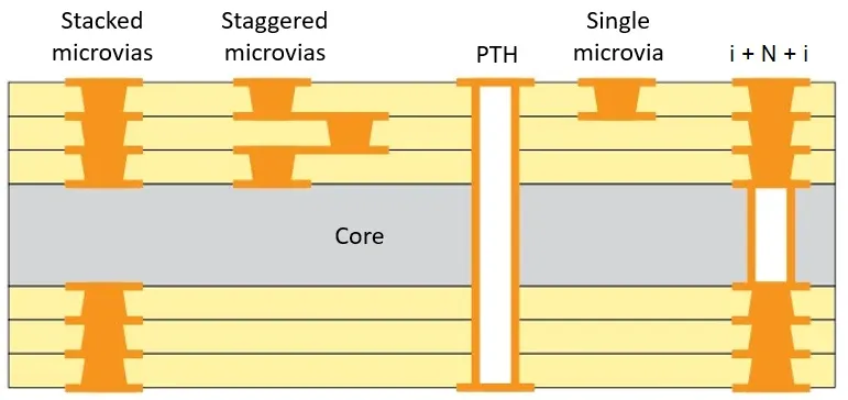
Industry standards often recommend keeping the aspect ratio between 6:1 and 10:1 for through-hole vias to ensure manufacturability. For microvias, which are smaller and used in high-density designs, the ratio should ideally be 1:1 or less to avoid plating challenges.
Understanding this calculation helps you design vias that are feasible to manufacture and reliable in operation. If the ratio is too high, you risk running into production issues or long-term reliability problems. Speaking of which, let's explore the challenges associated with high aspect ratios.
Common High Aspect Ratio Via Problems
Designing with a high via aspect ratio—where the board is much thicker than the via diameter—can introduce several issues that affect PCB via reliability. While high aspect ratios are sometimes necessary for complex, multi-layer boards, they come with risks that every designer should be aware of. Here are the most common high aspect ratio via problems:
- Plating Difficulties: When the via hole is too narrow relative to the board thickness (e.g., a ratio of 12:1), the electroplating solution struggles to flow evenly inside the via. This can result in insufficient copper deposition at the center of the via, creating weak spots.
- Thermal Stress: High aspect ratio vias are more prone to cracking under thermal expansion during soldering or operation. For instance, a via with a 15:1 ratio in a 2.4 mm thick board may experience stress that leads to barrel cracks, disrupting connectivity.
- Signal Integrity Issues: In high-frequency applications, uneven plating or structural flaws in high aspect ratio vias can cause impedance mismatches. This might result in signal reflections or losses, with impedance variations as high as 10-15% in poorly designed vias.
- Manufacturing Costs: Pushing the limits of aspect ratio often requires specialized drilling or plating processes, increasing production costs and lead times.
To mitigate these issues, designers should aim for moderate aspect ratios within the recommended range. If a high ratio is unavoidable, consider using advanced manufacturing techniques like laser drilling for microvias or consult with your fabrication partner to ensure process capability.
Via Plating Issues and Their Impact on Reliability
One of the most critical factors in PCB via reliability is the quality of copper plating inside the via. Via plating issues can turn a well-designed board into a failure waiting to happen. Let's look at the common plating problems and how they tie back to aspect ratio:
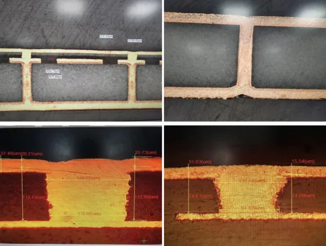
- Uneven Copper Deposition: In vias with high aspect ratios, the plating solution may not reach the middle of the hole, leading to thinner copper walls in the center. This creates weak points that can fail under mechanical or thermal stress.
- Voids in Plating: Air bubbles or contaminants trapped during plating can form voids—empty spaces in the copper layer. These voids reduce conductivity and can cause the via to overheat, with potential temperature rises of 20-30°C above normal during high-current operation.
- Insufficient Plating Thickness: Industry standards, such as IPC-6012, often require a minimum plating thickness of 20-25 micrometers for reliable vias. If the aspect ratio is too high, achieving this thickness becomes challenging, leading to poor electrical performance.
- Barrel Cracking: Poorly plated vias are more susceptible to cracking along the barrel (the cylindrical wall of the via). This is especially problematic in environments with temperature cycling, where expansion and contraction stress the via structure.
The key to avoiding these via plating issues lies in optimizing the aspect ratio during the design phase. Additionally, working with a manufacturing partner who uses advanced plating techniques, such as pulse plating, can improve copper distribution in challenging vias.
Best Practices for Optimizing Via Aspect Ratio
Now that we've covered the challenges, let's focus on actionable strategies to optimize via aspect ratio and enhance PCB via reliability. These best practices can help you avoid common pitfalls and ensure your design performs as intended.
1. Stick to Recommended Aspect Ratios
For through-hole vias, aim for an aspect ratio between 6:1 and 10:1. For microvias, keep the ratio at or below 1:1. These ranges balance manufacturability with performance, reducing the risk of plating or structural issues.
2. Adjust Board Thickness or Via Size
If your initial design results in a high aspect ratio, consider reducing the board thickness by using fewer layers or increasing the via diameter. For example, increasing a via diameter from 0.2 mm to 0.3 mm on a 1.6 mm board lowers the aspect ratio from 8:1 to 5.33:1, making plating easier.
3. Use Microvias for High-Density Designs
In boards with many layers or tight spacing, microvias with low aspect ratios can replace traditional through-hole vias. These smaller vias, often drilled with lasers, are ideal for high-density interconnects and have fewer plating challenges.
4. Simulate Thermal and Electrical Performance
Before finalizing your design, use simulation tools to test how vias will behave under thermal stress or high-frequency signals. For instance, ensure impedance remains within ±10% of your target value (e.g., 50 ohms for many RF applications) to avoid signal integrity issues.
5. Collaborate with Your Manufacturer
Every fabrication house has specific capabilities and limits for aspect ratios. Early communication with your manufacturing partner can help you tailor your design to their process, avoiding costly redesigns or production delays.
How Via Aspect Ratio Affects Different PCB Applications
The importance of via aspect ratio varies depending on the application of your PCB. Here's how it impacts different scenarios:
- High-Frequency Designs: In RF or microwave circuits, vias must maintain consistent impedance to prevent signal reflections. High aspect ratios can disrupt this, causing signal loss of up to 3-5 dB in extreme cases.
- Power Electronics: Boards handling high currents need robust vias to avoid overheating. Poorly plated vias with high aspect ratios may fail under loads as low as 2-3 amps, leading to burnout.
- Consumer Electronics: For compact devices with thin boards, microvias with low aspect ratios are often used to save space while maintaining reliability.
- Automotive and Aerospace: These industries demand vias that withstand extreme temperatures and vibrations. A moderate aspect ratio ensures vias remain intact even after 1,000+ thermal cycles between -40°C and 125°C.
Understanding your application's specific needs allows you to prioritize the right via design parameters, ensuring reliability across diverse conditions.
Conclusion: Mastering Via Aspect Ratio for Reliable PCBs
In the world of PCB design, small details can make a big difference. Via aspect ratio may not grab headlines, but it's truly the unsung hero of PCB via reliability. By mastering via aspect ratio calculation, addressing high aspect ratio via problems, and solving via plating issues, you can create boards that perform flawlessly and stand the test of time.
Start by calculating your via aspect ratio early in the design process and aim for recommended ranges like 6:1 to 10:1 for through-hole vias. Be mindful of the challenges that come with high ratios, such as plating defects or thermal stress, and use best practices to optimize your design. Whether you're working on high-frequency circuits or rugged automotive systems, a well-designed via can be the difference between success and failure.


