 ALLPCB


In the fast-paced world of electronics, ensuring clear and reliable signal transmission is critical, especially in complex designs with high-layer-count PCBs. If you're wondering how to achieve optimal high-layer count PCB signal integrity, the answer lies in careful stackup design, impedance control, and simulation. This blog post will guide you through the essentials of crafting PCB stackups that maintain signal integrity, diving deep into practical strategies and technical insights for engineers and designers. Whether you're working on high-speed digital circuits or intricate RF applications, understanding these principles can make or break your design's performance.
What Is Signal Integrity and Why Does It Matter in High-Layer-Count PCBs?
Signal integrity refers to the quality of an electrical signal as it travels through a printed circuit board (PCB). In simpler terms, it ensures that the signal remains clear and undistorted from its source to its destination. In high-layer-count PCBs—those with 8, 12, or even 20+ layers—maintaining signal integrity becomes increasingly challenging due to the complexity of routing, multiple power and ground planes, and potential interference.
Why is this important? Poor signal integrity can lead to data errors, signal delays, and even complete system failures. For instance, in high-speed designs like 5G telecommunications or advanced computing, a distorted signal can result in dropped connections or incorrect data processing. With high-layer-count PCBs often used in such critical applications, mastering signal integrity is non-negotiable.
The Role of PCB Stackup in High-Layer-Count Designs
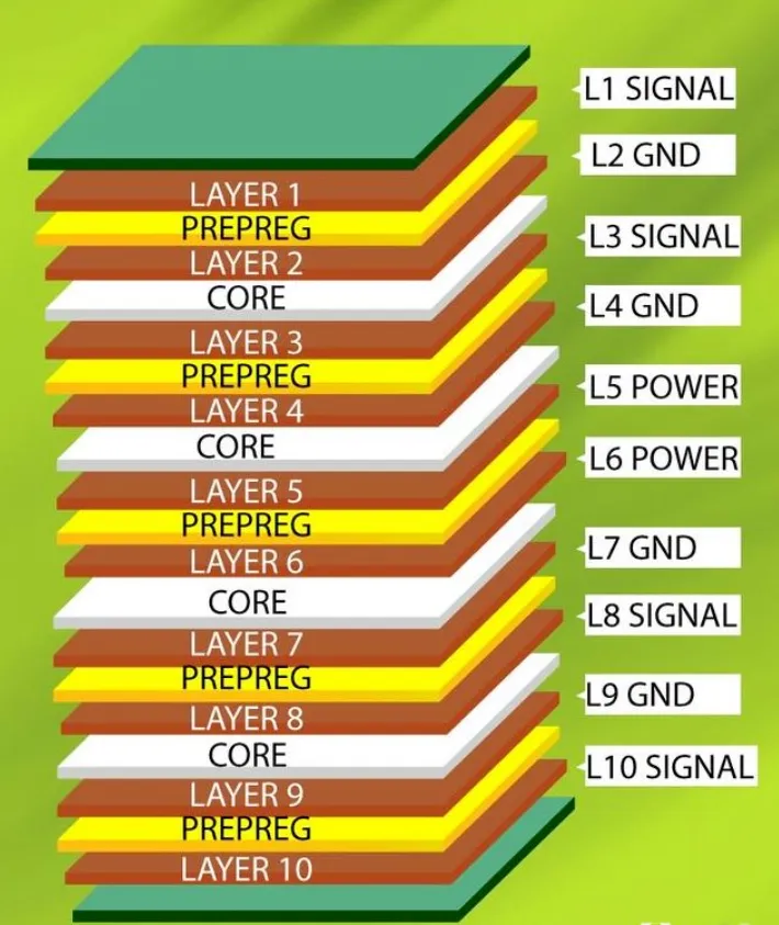
A PCB stackup is the arrangement of conductive and insulating layers in a board. In high-layer-count designs, the stackup directly impacts high-layer count PCB signal integrity by determining how signals interact with each other and their environment. A well-designed stackup minimizes crosstalk, controls impedance, and ensures efficient power distribution.
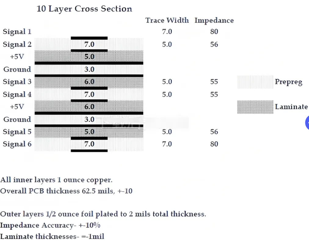
For example, a typical 12-layer PCB stackup might include multiple signal layers sandwiched between ground and power planes. The ground planes act as shields, reducing electromagnetic interference (EMI) between signal layers. The dielectric material between layers also plays a role, as its properties affect signal speed and impedance. A common dielectric like FR-4 has a permittivity (Dk) of around 4.2-4.5, which impacts how fast signals travel—typically at about 60-70% of the speed of light.
Designing the stackup requires balancing layer thickness, material choice, and layer order. An unbalanced stackup can lead to uneven thermal expansion, warping the board and degrading signal quality. Symmetry is key—ensuring that the stackup mirrors itself from the center outward helps maintain structural stability and consistent electrical performance.
Key Challenges in High-Layer-Count PCB Signal Integrity
High-layer-count PCBs introduce unique challenges that can compromise signal integrity if not addressed. Here are the primary hurdles designers face:
- Crosstalk: With more layers and denser routing, signals on adjacent traces or layers can interfere with each other. For instance, a signal switching at 5 GHz can induce noise in a nearby trace if not properly isolated by ground planes.
- Impedance Mismatches: Inconsistent impedance along a signal path causes reflections, distorting the signal. High-layer-count boards often have varied trace geometries across layers, making uniform impedance harder to achieve.
- Signal Delay and Skew: Longer traces or mismatched layer properties can delay signals, especially in differential pairs where timing is critical. A delay of just 10 picoseconds can disrupt high-speed data transmission at 10 Gbps.
- Power Distribution Issues: With multiple layers, ensuring stable power delivery becomes complex. Voltage drops or noise on power planes can affect signal quality across the board.
Addressing these challenges starts with a strategic approach to stackup design and impedance control, which we'll explore next.
Mastering PCB Stackup Impedance Control for Signal Integrity
Impedance control is a cornerstone of maintaining PCB stackup impedance control in high-layer-count designs. Impedance, measured in ohms, represents the resistance a signal encounters as it travels along a trace. For high-speed signals, matching the trace impedance to the source and load (often 50 ohms for RF or 100 ohms for differential pairs) is critical to prevent reflections.
How do you achieve this in a high-layer-count PCB? It starts with the stackup design. The impedance of a trace depends on its width, thickness, and the dielectric constant of the material surrounding it, as well as its proximity to reference planes (ground or power). For example, a microstrip trace on an outer layer over a ground plane might have a width of 6 mils to achieve 50 ohms impedance with a 4-mil dielectric thickness using FR-4 material.
In high-layer-count boards, where traces may be routed on internal layers as striplines (sandwiched between two reference planes), impedance calculations become more complex. Tools like impedance calculators or simulation software can help determine the exact trace dimensions needed. Additionally, maintaining consistent dielectric thickness across layers ensures uniform impedance, reducing mismatches.
Another tip is to avoid abrupt changes in trace geometry. For instance, transitioning a trace from one layer to another through a via can alter impedance if not carefully designed. Using back-drilling to remove unused via stubs or adding ground vias near signal vias can minimize these effects.
Leveraging Signal Integrity Simulation for High-Layer-Count PCBs
Designing a high-layer-count PCB without testing is like driving blindfolded. This is where signal integrity simulation high-layer PCB tools come into play. Simulation allows designers to model how signals behave in their stackup before manufacturing, identifying potential issues like crosstalk, reflections, or delays.
Modern simulation tools can analyze a PCB design in both frequency and time domains. For example, in the frequency domain, you can evaluate the impedance profile of a power distribution network (PDN) to ensure it meets a target impedance (often below 1 ohm for high-speed designs). In the time domain, simulations can reveal signal ringing or overshoot, which might occur if a signal switches at 2.5 GHz and encounters an impedance mismatch.
One practical application is simulating differential pairs, which are common in high-speed designs like USB 3.0 or PCIe. A simulation can check if the pair maintains a 100-ohm differential impedance and if skew between the positive and negative lines is within acceptable limits (typically under 15 picoseconds). If issues are found, you can adjust the stackup or routing before prototyping, saving time and cost.
Simulation also helps optimize via placement and layer transitions. For instance, a poorly placed via might introduce a 5% impedance discontinuity, leading to reflections. By simulating different via configurations, you can find the best layout for minimal signal disruption.
Best Practices for Designing High-Layer-Count PCB Stackups
Now that we've covered the fundamentals, let's dive into actionable best practices for designing stackups that ensure high-layer count PCB signal integrity. These tips are grounded in real-world design principles and can be applied to most high-speed projects.
1. Prioritize Ground and Power Planes
Place ground planes adjacent to signal layers to provide a low-impedance return path for signals. In a 16-layer board, for instance, dedicate at least 4-6 layers to ground and power to stabilize voltage and shield signals. Avoid splitting ground planes unless absolutely necessary, as splits can disrupt return paths and increase EMI.
2. Use Symmetrical Stackups
As mentioned earlier, symmetry prevents warping and maintains consistent electrical properties. For a 10-layer board, arrange layers so the top five mirror the bottom five in terms of material thickness and type. This balance also aids in manufacturing, reducing the risk of defects.
3. Control Dielectric Materials
Choose dielectric materials with consistent properties across layers. For high-speed designs, consider low-loss materials with a dielectric constant (Dk) below 3.5 to reduce signal attenuation. While these materials cost more than standard FR-4, they can improve performance in applications above 10 GHz.
4. Minimize Via Transitions
Each via introduces a potential point of signal degradation. Route signals on the same layer when possible, and use blind or buried vias for internal layer transitions to reduce stub effects. If full vias are unavoidable, back-drill them to remove unused portions.
5. Test and Iterate with Simulation
Always simulate your design before fabrication. Focus on critical nets, such as high-speed data lines or clock signals, and adjust the stackup or routing based on simulation feedback. This iterative approach ensures that issues are caught early.
Conclusion: Building Better PCBs with Signal Integrity in Mind
High-layer-count PCBs are at the heart of modern electronics, powering everything from data centers to telecommunications infrastructure. However, their complexity demands a meticulous approach to stackup design, PCB stackup impedance control, and signal integrity simulation high-layer PCB analysis. By prioritizing symmetry, controlling impedance, and leveraging simulation tools, you can unlock the full potential of your designs while ensuring reliable performance.
At ALLPCB, we understand the importance of signal integrity in high-layer-count designs. Our expertise and advanced manufacturing capabilities can help bring your complex PCB projects to life with precision and quality. Whether you're tackling a 12-layer board for a high-speed application or pushing the limits with a 24-layer design, the principles outlined in this guide will set you on the path to success.
Start applying these strategies in your next project, and watch as your designs achieve new levels of performance and reliability. With the right stackup and a focus on high-layer count PCB signal integrity, the possibilities are endless.


