 ALLPCB


If you're facing challenges with Electroless Nickel Immersion Gold (ENIG) finishes on your printed circuit boards (PCBs), you're not alone. ENIG is a popular surface finish due to its excellent solderability and durability, but it can come with issues like black pad, poor wetting, and weak solder joints. In this comprehensive guide, we'll walk you through common ENIG solderability problems, including ENIG black pad troubleshooting, ENIG wetting issues, ENIG poor solder joint formation, and ENIG solder paste compatibility. By the end, you'll have actionable solutions to ensure reliable PCB assembly and performance.
What is ENIG and Why Does It Matter?
ENIG, or Electroless Nickel Immersion Gold, is a widely used surface finish in PCB manufacturing. It consists of a layer of nickel deposited on the copper pads, topped with a thin layer of gold. This finish protects the copper from oxidation, provides a flat surface for soldering, and ensures good conductivity. ENIG is especially favored for its compatibility with fine-pitch components and its ability to withstand multiple reflow cycles, making it ideal for high-reliability applications like aerospace and medical devices.
However, despite its advantages, ENIG can present solderability challenges that impact the quality of solder joints and overall board performance. Issues like black pad, poor wetting, and compatibility problems with solder paste can lead to costly rework or product failures. Understanding these problems and knowing how to troubleshoot them is crucial for engineers and manufacturers aiming for consistent, high-quality results.
Common ENIG Solderability Problems
Before diving into troubleshooting, let’s identify the most frequent ENIG solderability issues that manufacturers encounter. Recognizing these problems early can save time and resources during production.
1. ENIG Black Pad: A Hidden Threat
One of the most notorious issues with ENIG is the "black pad" phenomenon. This occurs when the nickel layer underneath the gold becomes corroded during the immersion gold process, resulting in a brittle, non-solderable surface. Black pad often appears as dark or discolored patches on the pads and can lead to weak or failed solder joints.
The root cause of black pad is often linked to excessive phosphorus content in the nickel layer (typically above 10-11% by weight), which can make the nickel more prone to corrosion. Other contributing factors include improper control of the gold immersion bath or contamination during processing. This issue is particularly problematic because it may not be visible until soldering fails during assembly or testing.
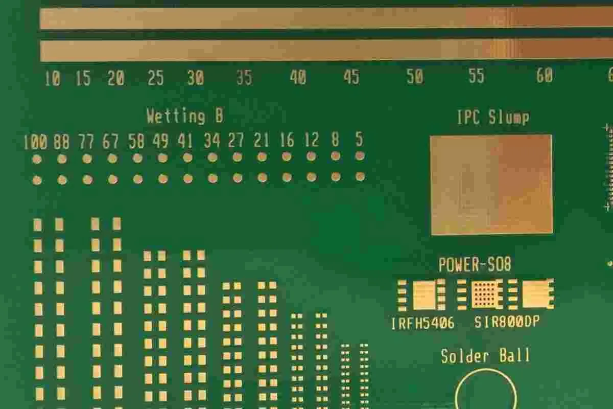
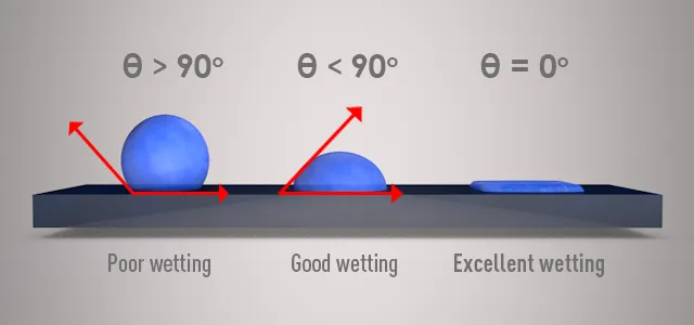
2. ENIG Wetting Issues: Why Solder Won’t Stick
Poor solder wetting is another common challenge with ENIG finishes. Wetting refers to the ability of molten solder to spread evenly across the pad surface. When wetting fails, the solder may form uneven or incomplete joints, leading to reliability issues. ENIG wetting issues often stem from surface contamination, oxidation of the nickel layer, or an overly thick gold layer (above 0.05-0.1 micrometers), which can interfere with solder adhesion.
Wetting problems can also be exacerbated by improper storage conditions. If ENIG-finished PCBs are exposed to high humidity or temperature fluctuations for extended periods (e.g., over 6 months), the surface may degrade, reducing solderability.
3. ENIG Poor Solder Joint Formation: Weak Connections
Weak or brittle solder joints are a direct consequence of issues like black pad or poor wetting. In ENIG poor solder joint formation, the solder may not bond properly with the nickel layer, resulting in joints that crack or fail under thermal or mechanical stress. This is often seen in applications with high thermal cycling, where temperature changes cause expansion and contraction of materials.
Studies have shown that solder joint failures in ENIG boards can increase by up to 30% if black pad or excessive phosphorus content is present. This statistic highlights the importance of addressing underlying issues during the manufacturing process to ensure robust connections.
4. ENIG Solder Paste Compatibility: Matching Materials
Not all solder pastes work well with ENIG finishes. ENIG solder paste compatibility issues arise when the flux or alloy composition in the paste doesn’t interact effectively with the gold or nickel layers. For instance, some lead-free solder pastes with high tin content (e.g., SAC305 alloy with 96.5% tin) may form intermetallic compounds with the nickel layer that are too brittle, leading to joint failures.
Additionally, the flux in the solder paste must be aggressive enough to remove any surface oxides or contaminants on the ENIG finish. If the flux is too mild, it may not clean the surface properly, resulting in poor wetting and weak joints.
Troubleshooting ENIG Solderability Issues
Now that we’ve identified the common problems, let’s explore practical solutions for troubleshooting ENIG solderability issues. These steps are designed to help you diagnose and resolve issues during design, manufacturing, and assembly stages.
Step 1: Diagnosing ENIG Black Pad
Identification: Black pad is often invisible to the naked eye until soldering fails. Use a microscope to inspect pads for discoloration or dark spots after soldering. Cross-sectional analysis can reveal corrosion at the nickel-gold interface. Testing for phosphorus content using Energy Dispersive X-ray (EDX) analysis can also confirm if levels exceed the safe range of 7-9%.
Solution: To prevent black pad, work with your PCB fabricator to ensure tight control over the ENIG plating process. This includes maintaining proper pH levels (around 4.5-5.0) in the gold immersion bath and minimizing contamination. Specifying a lower phosphorus content in the nickel layer (targeting 7-8%) can also reduce corrosion risks. If black pad is detected on finished boards, affected pads may need to be reworked or replaced, though this can be costly.
Step 2: Addressing ENIG Wetting Issues
Identification: Poor wetting is evident when solder beads up or fails to spread across the pad during reflow. Inspect joints visually or use automated optical inspection (AOI) to detect non-wetted areas. Storage conditions should also be reviewed—boards stored for over 6 months may show reduced solderability due to surface degradation.
Solution: Ensure proper cleaning of PCBs before soldering to remove contaminants like fingerprints or dust. Use a mild solvent or plasma cleaning if necessary. Control the gold layer thickness to stay within 0.05-0.1 micrometers, as thicker layers can hinder wetting. For long-term storage, package boards in vacuum-sealed bags with desiccants to protect against humidity (ideal storage humidity is below 50% RH).
Step 3: Fixing ENIG Poor Solder Joint Formation
Identification: Weak solder joints can be identified through visual inspection (cracks or incomplete fillets) or by conducting thermal cycling tests. A pull-test or shear-test can quantify joint strength—joints failing below 5-7 pounds of force indicate potential issues with the ENIG finish.
Solution: Address underlying causes like black pad or wetting issues using the steps above. Optimize the reflow profile to ensure adequate heat (peak temperatures of 235-245°C for lead-free solder) and time above liquidus (60-90 seconds) to form strong intermetallic bonds. If joints remain weak, consider switching to a different surface finish for critical applications, though this should be a last resort due to design changes.
Step 4: Ensuring ENIG Solder Paste Compatibility
Identification: Compatibility issues manifest as poor wetting or brittle joints during assembly. Review the solder paste datasheet to check its flux type (e.g., no-clean, water-soluble) and alloy composition. Test samples on ENIG boards to observe joint quality before full-scale production.
Solution: Select a solder paste with a flux that matches ENIG characteristics. For instance, a mildly activated rosin (RMA) flux often works well with ENIG by effectively cleaning the surface. Avoid overly aggressive fluxes that can corrode the gold layer. If using lead-free solder, ensure the alloy (e.g., SAC305) is compatible with nickel intermetallic formation—consult with your paste supplier for recommendations. Stencil design also matters; use a stencil thickness of 0.1-0.15 mm to apply the right amount of paste for consistent results.
Preventive Measures for Long-Term Success
Troubleshooting is essential, but prevention is even better. Here are proactive steps to minimize ENIG solderability problems during design and manufacturing:
- Collaborate with Fabricators: Work closely with your PCB manufacturer to define strict ENIG process parameters, such as nickel phosphorus content (7-9%) and gold thickness (0.05-0.1 micrometers).
- Specify Testing: Request incoming quality control tests, such as solderability testing per IPC-J-STD-003 standards, to verify ENIG performance before assembly.
- Optimize Storage: Store ENIG-finished boards in controlled environments (temperature 20-25°C, humidity below 50% RH) to maintain surface integrity.
- Review Assembly Processes: Ensure reflow ovens are calibrated for consistent heating, and use nitrogen atmospheres if oxidation is a concern during soldering.
Conclusion: Mastering ENIG for Reliable PCBs
ENIG remains a top choice for PCB surface finishes due to its durability and versatility, but it’s not without challenges. By understanding and addressing common ENIG solderability problems like black pad, wetting issues, poor solder joint formation, and solder paste compatibility, you can achieve reliable, high-quality assemblies. Use the troubleshooting steps and preventive measures outlined in this guide to tackle issues head-on and optimize your manufacturing process.
Whether you’re an engineer designing complex boards or a manufacturer aiming for zero-defect production, mastering ENIG troubleshooting is a valuable skill. With careful attention to process control, material selection, and assembly techniques, you can minimize failures and ensure your PCBs perform as intended in even the most demanding applications.


