 ALLPCB


In the world of PCB manufacturing, through-hole via filling and plugging are specialized techniques that can significantly impact the performance, reliability, and longevity of a printed circuit board (PCB). But when should you use via filling or plugging, and why are these processes important? Simply put, via filling and plugging are used to enhance the structural integrity, thermal management, and electrical performance of PCBs, especially in high-density or high-reliability applications. These methods prevent issues like air entrapment, improve soldering quality, and protect against environmental damage, making them essential for modern electronics.
In this detailed guide, we’ll explore the ins and outs of via filling and via plugging, including the differences between conductive and non-conductive via fill, the role of via tenting, and the specific scenarios where these techniques are most beneficial. Whether you’re designing a complex multilayer board or looking to optimize a simple prototype, understanding these processes will help you make informed decisions for your next project.
What Are Through-Hole Vias in PCB Manufacturing?
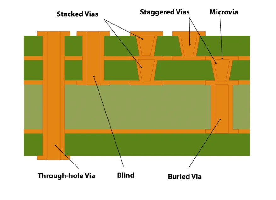
Before diving into via filling and plugging, let’s clarify what a through-hole via is. In PCB manufacturing, a via is a small hole drilled through the board to connect different layers electrically. Through-hole vias, specifically, pass through the entire thickness of the PCB, from the top layer to the bottom layer. These vias are typically plated with a conductive material, like copper, to ensure a reliable electrical connection between layers.
Vias are critical in multilayer PCBs, where space is limited, and complex routing is required. However, unfilled or unprotected vias can pose challenges, such as air or moisture entrapment, poor soldering results, or even structural weaknesses. This is where via filling and plugging come into play, addressing these potential issues and enhancing the overall performance of the board.
What Is Via Filling and Why Does It Matter?
Via filling is a process in PCB manufacturing where the through-hole vias are filled with a material—either conductive or non-conductive—to eliminate empty space inside the hole. This technique is often used in high-density interconnect (HDI) boards or multilayer designs where reliability and performance are critical.
The primary reasons for via filling include:
- Preventing Air or Liquid Entrapment: Empty vias can trap air or liquids during the soldering process, leading to defects like voids or cracks. Filling the via reduces this risk, ensuring a more robust assembly.
- Improving Thermal Dissipation: Conductive via fill materials, such as copper or silver epoxy, enhance heat transfer through the via, helping to manage thermal loads in high-power applications. For instance, a filled via can reduce thermal resistance by up to 30% compared to an unfilled via in some designs.
- Enhancing Mechanical Strength: Filling a via adds structural support to the PCB, reducing the risk of cracking or delamination under mechanical stress.
- Supporting Stacked Vias: In HDI designs, filled vias provide a flat surface for stacking additional vias on top, enabling more compact and complex layouts.
Via filling is particularly important in applications like automotive electronics, aerospace systems, and medical devices, where failure is not an option. By addressing potential weak points in the PCB, this process ensures long-term reliability under harsh conditions.
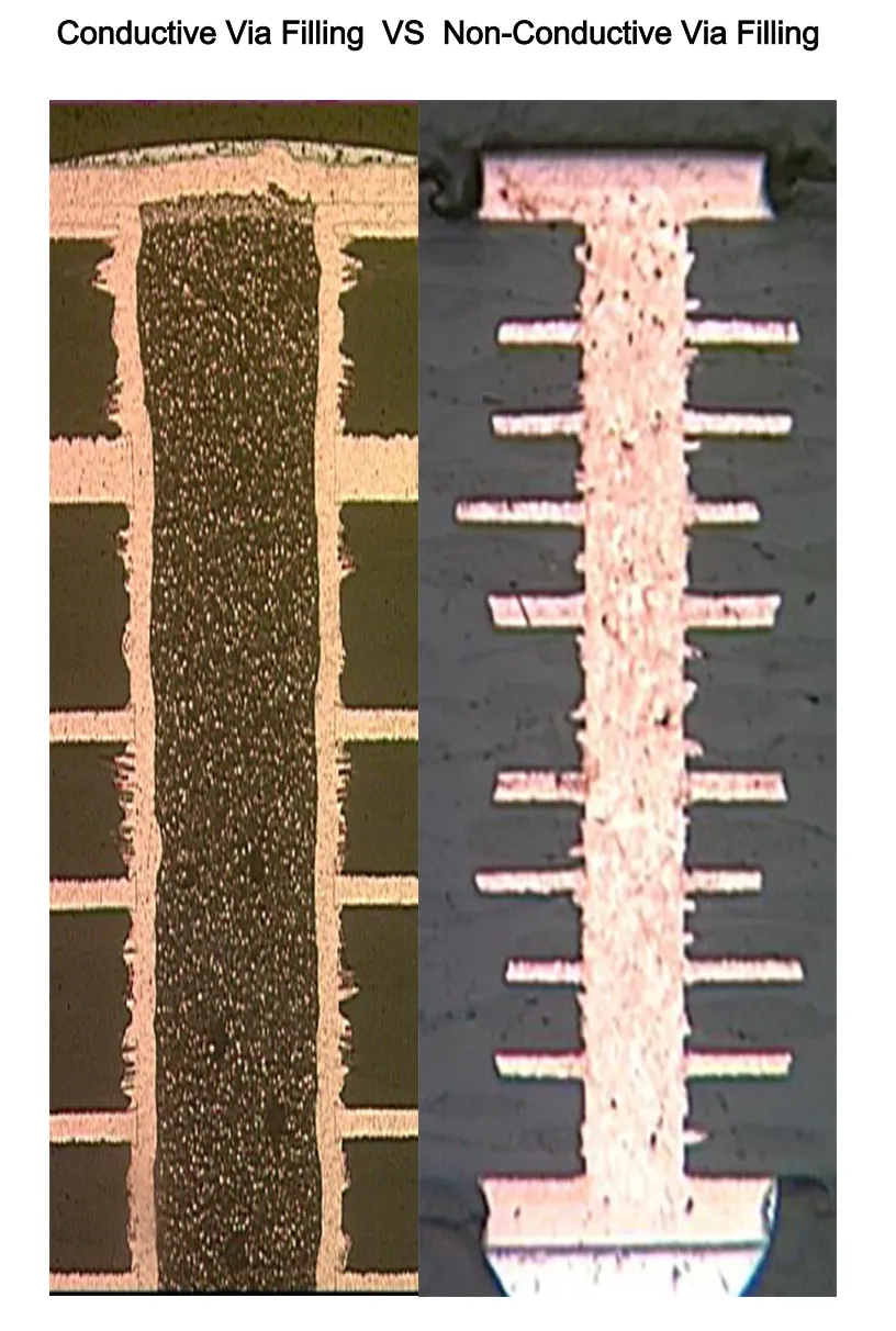
Conductive vs. Non-Conductive Via Fill: Which to Choose?
When it comes to via filling, you have two main options: conductive via fill and non-conductive via fill. Each has distinct properties and use cases, so understanding their differences is key to selecting the right approach for your design.
Conductive Via Fill
Conductive via fill involves filling the via with a material that conducts electricity, such as copper paste or silver epoxy. This method is ideal for applications where both electrical and thermal conductivity are priorities.
- Benefits: Enhances electrical performance by reducing impedance (often below 1 ohm for small vias) and improving signal integrity. It also boosts thermal conductivity, making it suitable for high-power designs.
- Applications: Commonly used in power electronics, LED lighting boards, and RF circuits where heat dissipation and low signal loss are critical.
- Drawbacks: Conductive fill materials are typically more expensive and may require additional processing steps during manufacturing.
Non-Conductive Via Fill
Non-conductive via fill uses materials like epoxy resin that do not conduct electricity. This option focuses on structural and environmental protection rather than electrical performance.
- Benefits: Provides excellent protection against moisture and contaminants, improves mechanical stability, and is generally more cost-effective than conductive fill.
- Applications: Ideal for standard multilayer PCBs, consumer electronics, and designs where thermal or electrical conductivity through the via is not a priority.
- Drawbacks: Does not contribute to thermal management or electrical performance, limiting its use in high-performance applications.
Choosing between conductive and non-conductive via fill depends on the specific needs of your PCB. For high-frequency designs operating at speeds above 1 GHz, conductive fill may be necessary to maintain signal integrity. For simpler designs, non-conductive fill often provides sufficient protection at a lower cost.
What Is Via Plugging and How Does It Differ from Filling?
While via filling involves completely filling the via hole with material, via plugging is a related but distinct process. Via plugging typically refers to sealing the via opening on one or both sides of the PCB with a material like solder mask or epoxy, rather than filling the entire hole. The goal of plugging is often to protect the via from external contaminants or to prevent solder from flowing into the via during assembly.
Key aspects of via plugging include:
- Protection: Plugging prevents dust, moisture, or chemicals from entering the via, which is especially important in harsh environments.
- Solder Flow Control: During soldering, plugging stops molten solder from wicking into the via, which can cause uneven joints or shorts.
- Cost-Effectiveness: Plugging is often less expensive than full via filling, as it uses less material and requires fewer manufacturing steps.
However, via plugging does not provide the same level of structural support or thermal benefits as via filling, since the interior of the via remains empty. It’s a suitable choice for designs where environmental protection is the primary concern, but high mechanical or thermal demands are not present.
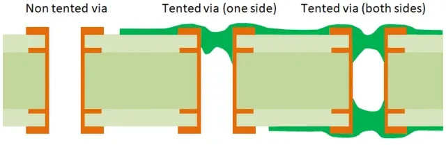
The Role of Via Tenting in PCB Manufacturing
Another technique related to via protection is via tenting. Via tenting involves covering the via opening with a layer of solder mask, leaving the via hole itself unfilled. This method is simpler and more cost-effective than filling or plugging, making it a popular choice for less demanding applications.
Benefits of via tenting include:
- Corrosion Resistance: The solder mask layer shields the via from environmental factors like humidity or chemicals, reducing the risk of corrosion.
- Reduced Solder Wicking: Tenting prevents solder from flowing into the via during assembly, ensuring cleaner and more reliable solder joints.
- Cost Savings: Since no additional materials are used to fill or plug the via, tenting is an economical option for standard PCB designs.
Via tenting is best suited for smaller vias (less than 15 mils in diameter) in non-critical applications. For larger vias or high-reliability designs, filling or plugging may be necessary to provide adequate protection and performance.
When Should You Use Via Filling or Plugging?
Deciding whether to use via filling, plugging, or tenting depends on the specific requirements of your PCB design. Here are some scenarios where these techniques are most beneficial:
- High-Density Designs: In HDI boards with tight spacing and stacked vias, via filling (especially conductive fill) is often necessary to ensure reliable connections and support complex routing. For example, a 10-layer HDI board with via-in-pad designs may require filling to maintain a flat surface for component placement.
- Harsh Environments: For PCBs used in automotive, aerospace, or industrial applications, via plugging or filling with non-conductive materials can protect against moisture, dust, and temperature extremes, extending the board’s lifespan.
- High-Power Applications: If your design involves significant heat generation, such as in power supply circuits, conductive via fill can improve thermal dissipation, preventing overheating and potential failure.
- Standard Consumer Electronics: For less demanding applications, via tenting or simple plugging with solder mask may be sufficient to provide basic protection without adding unnecessary cost.
Ultimately, the choice comes down to balancing performance needs with budget constraints. Collaborating with your PCB manufacturer early in the design process can help determine the most suitable approach for your project.
Benefits of Via Filling and Plugging in PCB Manufacturing
Implementing via filling or plugging offers several advantages that directly impact the quality and reliability of your PCB. Some of the key benefits include:
- Enhanced Reliability: By eliminating voids and protecting against environmental damage, these techniques reduce the likelihood of failures, even in challenging conditions.
- Better Signal Integrity: Conductive via fill minimizes impedance mismatches and signal loss, supporting high-speed designs with frequencies exceeding 5 GHz in some cases.
- Improved Assembly Quality: Filled or plugged vias prevent solder-related defects, leading to more consistent and durable solder joints during assembly.
- Longer Lifespan: Protection against moisture, corrosion, and mechanical stress extends the operational life of the PCB, reducing maintenance and replacement costs.
These benefits make via filling and plugging indispensable for modern PCB designs, especially as electronics become smaller, faster, and more complex.
Challenges and Considerations in Via Filling and Plugging
While via filling and plugging offer significant advantages, there are also challenges to keep in mind during the design and manufacturing process:
- Cost: Conductive via fill, in particular, can increase manufacturing costs due to the materials and additional processing steps involved. Non-conductive fill and plugging are more budget-friendly but may not meet all performance needs.
- Manufacturing Complexity: Filling vias, especially in high-density designs, requires precision to avoid incomplete fills or voids, which can compromise reliability.
- Design Constraints: Filled or plugged vias may affect the flexibility of your design, as they can limit future modifications or rework options.
To mitigate these challenges, ensure that your design files clearly specify the type of via protection required, and work closely with your manufacturing partner to optimize the process for cost and quality.
How to Specify Via Filling and Plugging in Your PCB Design
To achieve the desired results with via filling or plugging, clear communication with your PCB manufacturer is essential. Here are some tips for specifying these processes in your design:
- Include Detailed Notes: Clearly indicate which vias require filling, plugging, or tenting in your design documentation. Specify the material (conductive or non-conductive) if applicable.
- Use Industry Standards: Reference standards like IPC-4761, which provides guidelines for via protection, to ensure consistency and compatibility with manufacturing capabilities.
- Verify Design Rules: Check that your design adheres to the manufacturer’s design rules for via size, spacing, and fill material to avoid production issues.
By providing precise instructions and collaborating with your manufacturer, you can ensure that via filling or plugging is implemented effectively in your PCB.
Conclusion: Making the Right Choice for Your PCB
Through-hole via filling and plugging are powerful techniques in PCB manufacturing that address critical challenges related to reliability, performance, and environmental protection. Whether you opt for conductive via fill to enhance thermal and electrical performance, non-conductive fill for cost-effective protection, or via plugging for environmental sealing, understanding the specific needs of your design is key to making the right choice.
By considering factors like application requirements, environmental conditions, and budget constraints, you can select the most appropriate via protection method for your project. With the right approach, via filling, plugging, or tenting can elevate the quality of your PCB, ensuring it performs reliably in even the most demanding scenarios.


