 ALLPCB


Designing a printed circuit board (PCB) requires precision, especially when it comes to determining the right trace width. If you're searching for a reliable way to calculate trace width, a PCB trace width calculator is your go-to tool. Whether you're focusing on current capacity, temperature rise, or compliance with standards like IPC-2221, this guide will walk you through everything you need to know. We'll explore how to use an online PCB trace width calculator, account for current and temperature factors, and ensure your design is safe and efficient.
In this comprehensive guide, we'll break down the importance of trace width, the role of standards like IPC-2221, and how calculators simplify the process. By the end, you'll have actionable insights to apply in your next PCB design project.
Why PCB Trace Width Matters in Design
PCB trace width is a critical factor in ensuring your circuit board functions safely and reliably. Traces are the thin copper lines on a PCB that carry electrical current between components. If a trace is too narrow for the current it carries, it can overheat, leading to potential damage or failure. On the other hand, overly wide traces waste valuable board space and increase manufacturing costs.
The goal is to find the perfect balance. A well-calculated trace width ensures that current flows without excessive heat buildup, maintains signal integrity, and adheres to design constraints. This is where tools like a PCB trace width calculator for current or a PCB trace width calculator temperature come into play, helping you make informed decisions based on your specific requirements.

Understanding the IPC-2221 Standard for Trace Width
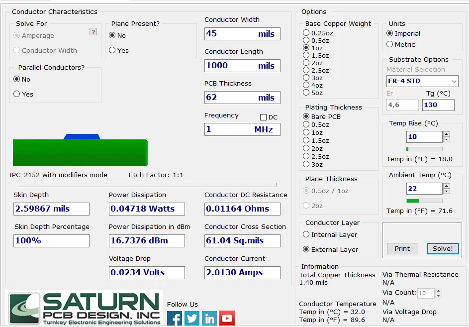
The IPC-2221 standard is a widely recognized guideline in the electronics industry for designing PCBs. It provides detailed recommendations on trace width based on the current a trace must carry and the acceptable temperature rise. Using a PCB trace width calculator IPC-2221 ensures your design aligns with these proven standards, reducing the risk of overheating or electrical failure.
According to IPC-2221, trace width calculations depend on factors like:
- Current Load: The amount of current (in amperes) the trace will carry.
- Temperature Rise: The acceptable increase in temperature (in degrees Celsius) above ambient conditions, often set between 10°C and 20°C for most designs.
- Copper Thickness: Measured in ounces per square foot (oz/ft2), typically 1 oz/ft2 or 2 oz/ft2, which affects how much current a trace can handle.
- Ambient Temperature: The surrounding temperature where the PCB operates, impacting heat dissipation.
While IPC-2221 offers detailed charts and formulas, manually calculating trace width can be time-consuming and prone to errors. This is why many designers turn to digital tools that incorporate these standards for quick and accurate results.
How a PCB Trace Width Calculator Works
An online PCB trace width calculator simplifies the complex calculations needed to determine the appropriate trace width. These tools use formulas derived from standards like IPC-2221 or the updated IPC-2152, which focuses more on real-world testing for current-carrying capacity.
Here's how most calculators operate:
- Input Parameters: You enter details such as the current (e.g., 2.5 A), desired temperature rise (e.g., 10°C), copper thickness (e.g., 1 oz/ft2), and ambient temperature (e.g., 25°C).
- Calculation: The tool processes these inputs using established equations to estimate the minimum trace width required.
- Output: You receive a recommended trace width (in mils or millimeters) to ensure safe current flow without excessive heating.
Some calculators also account for whether the trace is on an internal or external layer of the PCB, as heat dissipation varies based on location. External traces cool more effectively due to exposure to air, while internal traces may require wider dimensions to manage heat.
Key Factors in Calculating PCB Trace Width
When using a PCB trace width calculator for current or temperature considerations, understanding the influencing factors is essential. Let's dive into the main elements that affect trace width calculations.
1. Current Capacity
The amount of current a trace carries is the primary determinant of its width. Higher currents require wider traces to prevent overheating. For example, a trace carrying 1 A might need a width of 10 mils (0.254 mm) at 1 oz/ft2 copper thickness with a 10°C temperature rise. However, for 5 A, the width could increase to 50 mils (1.27 mm) under the same conditions.
2. Temperature Rise
Temperature rise refers to how much hotter the trace gets compared to the surrounding environment. A PCB trace width calculator temperature feature helps you set a safe limit. For instance, a 10°C rise is often used for general-purpose designs, while high-power applications might allow a 20°C rise if heat dissipation is managed through other means like heat sinks.
3. Copper Thickness
Copper thickness impacts how much current a trace can handle for a given width. Thicker copper (e.g., 2 oz/ft2) allows for narrower traces compared to thinner copper (e.g., 0.5 oz/ft2) for the same current load. Most calculators let you select the copper weight to refine the results.
4. Trace Location
Traces on external layers dissipate heat better than those on internal layers due to air exposure. If your design includes multilayer boards, ensure the calculator accounts for trace location or adjust the temperature rise input accordingly.
5. Voltage Drop
Although not always a primary input in calculators, voltage drop across a trace can affect performance, especially in power delivery circuits. Wider traces reduce resistance and minimize voltage drop, ensuring components receive the intended voltage.
Benefits of Using an Online PCB Trace Width Calculator
Manually calculating trace width using charts or formulas can be tedious and error-prone. An online PCB trace width calculator offers several advantages for engineers and hobbyists alike:
- Speed: Get results in seconds by entering a few parameters.
- Accuracy: Built-in algorithms based on standards like IPC-2221 reduce the risk of miscalculation.
- Accessibility: Most tools are free and available online, requiring no specialized software.
- Customization: Adjust inputs like temperature rise or copper thickness to match your design needs.
These tools are especially helpful for beginners who may not yet fully understand the underlying math or for experienced designers working on tight deadlines.
Step-by-Step Guide to Using a PCB Trace Width Calculator
Ready to calculate the trace width for your next project? Follow these steps using any reliable online PCB trace width calculator:
- Gather Design Data: Determine the current your trace will carry, the acceptable temperature rise, copper thickness, and whether the trace is internal or external.
- Access a Calculator: Visit a trusted online tool that supports IPC-2221 or IPC-2152 standards.
- Enter Parameters: Input the values you collected. For example, set current to 3 A, temperature rise to 15°C, copper thickness to 1 oz/ft2, and select "external trace."
- Review Results: The calculator will output a trace width, such as 20 mils (0.508 mm). Double-check the inputs if the result seems unreasonable.
- Apply to Design: Use the calculated width in your PCB design software, ensuring it fits within your board's space constraints.
- Validate: If possible, simulate or prototype the design to confirm that the trace width handles the current without overheating.
Common Mistakes to Avoid in Trace Width Calculation
Even with a calculator, errors can occur if inputs or assumptions are incorrect. Here are some pitfalls to watch out for:
- Underestimating Current: Always account for peak current, not just average, to avoid undersizing traces.
- Ignoring Temperature Rise: Setting an unrealistic temperature rise can lead to overheating. Stick to conservative values like 10°C unless your design includes enhanced cooling.
- Forgetting Layer Location: Internal traces need wider dimensions than external ones due to limited heat dissipation.
- Neglecting Manufacturing Limits: Ensure the calculated trace width is feasible for your fabrication process. Some manufacturers have minimum width constraints (e.g., 6 mils).
Related Reading: Minimum Trace Width for Manufacturability: Avoiding PCB Fabrication Issues
Advanced Tips for High-Current and High-Temperature Designs
For designs involving high currents or extreme temperatures, standard calculations may not suffice. Consider these advanced strategies:
- Use Thicker Copper: Opt for 2 oz/ft2 or higher copper weight to reduce trace width while maintaining current capacity.
- Add Thermal Vias: Place vias near high-current traces to transfer heat to other layers or a heat sink.
- Increase Board Thickness: Thicker boards can handle more heat and may allow for narrower traces in some cases.
- Simulate Heat Distribution: Use thermal simulation software to predict temperature rise beyond calculator estimates, especially for complex designs.
Comparing IPC-2221 and IPC-2152 Standards
While IPC-2221 is the traditional standard for trace width calculations, IPC-2152 offers a more modern approach based on extensive testing. Here's a quick comparison:
- IPC-2221: Relies on theoretical models and charts, often resulting in conservative (wider) trace widths. It's widely supported in calculators and easy to use.
- IPC-2152: Uses empirical data from real-world tests, often yielding narrower trace widths for the same conditions. It accounts for more variables like board material and environment.
Many modern PCB trace width calculator IPC-2221 tools also incorporate IPC-2152 data, allowing you to choose the standard that best fits your project. For critical applications, IPC-2152 may provide more accurate results, but always consult your design requirements and manufacturer guidelines.
Conclusion: Mastering PCB Trace Width for Safe Designs
Calculating the correct trace width is a fundamental step in PCB design to ensure safe current flow and prevent overheating. By using an online PCB trace width calculator, you can save time and reduce errors while adhering to trusted standards like IPC-2221 or IPC-2152. Whether you're focusing on current capacity with a PCB trace width calculator for current or managing heat with a PCB trace width calculator temperature tool, the process becomes straightforward with the right resources.
Remember to consider factors like current load, temperature rise, copper thickness, and trace location when designing your board. Avoid common mistakes by double-checking inputs and validating results through simulation or prototyping. With these insights and tools at your disposal, you're well-equipped to create reliable and efficient PCB designs for any application.
Start leveraging a trace width calculator today to optimize your next project and ensure long-lasting performance.


